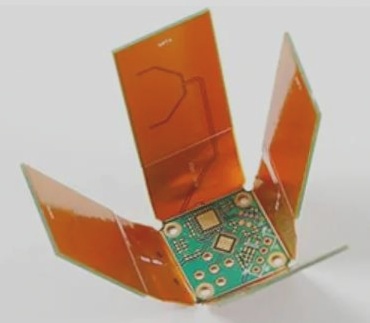
Essential Wiring Guidelines for USB 2.0 Devices
USB, a cost-effective and user-friendly hot-swappable serial interface, is widely utilized for its fast, bidirectional, and synchronous data transmission capabilities. However, many encounter issues with USB interfaces post-PCB assembly, leading to unstable communication or complete failure. To address these challenges, meticulous attention must be paid to the layout and design of the PCB, particularly concerning the differential signal lines essential for USB operation.
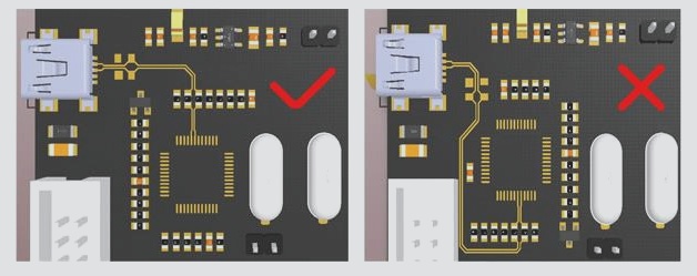
- Keep the length of the differential line minimal during component layout to reduce routing distance.
- Prioritize the layout of differential lines, avoiding excessive vias and ensuring symmetrical placement when necessary.
- Implement symmetrical parallel wiring techniques, opting for arc or 45° wiring to enhance signal integrity.
- Strategically place differential series connection components and consider factors like pin distribution and routing space to avoid mismatched line lengths.
- Maintain a distance of at least 20mil between other signal networks and the ground differential line to reduce crosstalk.
- Ensure appropriate line width for VBUS and GND to meet current carrying requirements and enhance power supply integrity.
For USB devices operating at 480 Mbits/s, controlling the impedance of the differential signal is crucial to maintain signal integrity. Parameters such as line width, dielectric constant, spacing, and distance to the reference layer influence impedance and impact signal quality. Adhering to principles like shortest length, tight coupling, equal length, and consistent impedance is paramount for successful USB device operation.