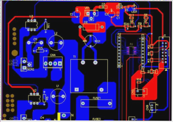
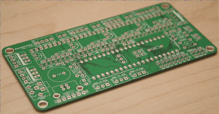
When designing a PCB (printed circuit board), one fundamental issue to consider is the number of wiring layers, ground planes, and power planes necessary to achieve the circuit’s required functions. The determination of these layers is influenced by factors such as circuit functionality, signal integrity, EMI, EMC, and manufacturing costs. In most designs, conflicting requirements arise among PCB performance, target costs, manufacturing capabilities, and system complexity. Therefore, the PCB laminate design typically results from a compromise after evaluating these various factors. High-speed digital and radio circuits generally utilize multi-layer board designs.
The following are the 8 principles to consider in cascading design:
1. Stratification
In a multi-layer PCB, it typically consists of a signal layer (S), a power (P) plane, and a ground (GND) plane. The power and ground planes are usually solid and undivided, providing an effective low-impedance return path for currents from adjacent signal traces. The signal layer is primarily situated between these power or ground reference plane layers, forming either a symmetrical or asymmetrical stripline. The top and bottom layers of a multilayer PCB are generally designated for component placement and a limited number of traces. These signal traces should be kept short to minimize direct radiation emitted by the traces.

2. Determine the single power reference plane (power plane)
Using decoupling capacitors is crucial for addressing power integrity issues. These capacitors can only be placed on the top and bottom layers of the PCB. The traces, pads, and vias associated with these capacitors can significantly impact their effectiveness. Therefore, it is essential to design the traces connecting the decoupling capacitors to be as short and wide as possible, while also keeping the vias’ connecting wires short. For instance, in a high-speed digital circuit, the decoupling capacitor can be placed on the top layer, designating the second layer for the high-speed digital circuit (like a processor) as the power layer, the third layer for signals, and the fourth layer as the ground for the high-speed digital circuit. Additionally, ensure that the signal traces driven by the same high-speed digital device share the same power layer as the reference plane.
3. Determine the multi-power reference plane
The multi-power reference plane will be segmented into several physical areas with different voltage levels. If a signal layer is in proximity to the multi-power supply layer, the signal current in that layer may encounter undesirable return paths, leading to gaps. For high-speed digital signals, poorly designed return paths can result in serious issues, necessitating that high-speed digital signal routing remains distant from the multi-power reference plane.
4. Determine multiple ground reference planes (ground planes)
Multiple ground reference planes can provide a low-impedance return path, effectively reducing common-mode EMI. The ground plane should be tightly coupled with the power plane, and the signal layer should also maintain close coupling with its adjacent reference plane. This can be achieved by minimizing the dielectric thickness between layers.
5. Reasonably design the wiring combination
The two layers connected by a signal path are referred to as a “wiring combination.” An optimal design avoids return currents flowing between different reference planes; instead, they should flow from one point on a reference plane to another point on the same plane. Complex routing may necessitate layer-to-layer trace conversions, so ensure smooth return current flow when transitioning between signal layers. Using adjacent layers as a wiring combination is generally reasonable, but spanning multiple layers for a signal path is often inefficient, as it disrupts return current flow. While placing decoupling capacitors near vias or reducing dielectric thickness can mitigate ground bounce, this is not an ideal design approach.
6. Set the wiring direction
Within the same signal layer, most wiring directions should be consistent and orthogonal to the directions of adjacent signal layers. For example, one signal layer might follow the “Y-axis” direction, while an adjacent layer could be set along the “X-axis.”
7. Adopt even-numbered layer structure
Analysis of PCB designs reveals that classic stack configurations typically feature even-numbered layers, not odd. This trend arises from various factors. The manufacturing process dictates that all conductive layers are contained within the core layer, which is usually a double-sided substrate. When fully utilized, this results in an even number of conductive layers.
Even-numbered boards offer cost benefits; although odd-numbered boards have slightly lower raw material costs, they incur higher processing costs due to the need for non-standard lamination processes. This adds complexity, potentially lowering production efficiency and extending production times. Additional processing on outer core layers increases the risk of defects, thereby raising manufacturing costs.
During multilayer bonding, differing lamination tensions may lead to varying degrees of bending, with odd-numbered boards being more prone to this issue. In contrast, even-numbered boards can mitigate bending risks.
When designing with an odd number of layers, consider these methods to increase the layer count. If the power supply layer is even and the signal layer is odd, adding a signal layer can enhance quality without increasing costs. Conversely, for an odd number of power layers and an even number of signal layers, consider adding a power layer. Another straightforward method is to insert a ground layer in the stack, allowing for the design to proceed on an odd-numbered layer while simply duplicating the ground layer in the middle.
In microwave circuits and mixed media designs, a blank signal layer may be inserted near the center of the stack to minimize imbalance.
8. Cost considerations
Regarding manufacturing costs, multi-layer circuit boards inherently carry higher expenses than single or double-layer boards, with costs increasing as the number of layers grows. However, when assessing circuit functionality, miniaturization, and performance indicators like signal integrity, EMI, and EMC, multi-layer boards should be prioritized. A comprehensive evaluation reveals that the cost difference between multi-layer and single-layer boards is often less than anticipated.
—
Let me know if you need further adjustments!
The following are the 8 principles to consider in cascading design:
1. Stratification
In a multi-layer PCB, it typically consists of a signal layer (S), a power (P) plane, and a ground (GND) plane. The power and ground planes are usually solid and undivided, providing an effective low-impedance return path for currents from adjacent signal traces. The signal layer is primarily situated between these power or ground reference plane layers, forming either a symmetrical or asymmetrical stripline. The top and bottom layers of a multilayer PCB are generally designated for component placement and a limited number of traces. These signal traces should be kept short to minimize direct radiation emitted by the traces.
2. Determine the single power reference plane (power plane)
Using decoupling capacitors is crucial for addressing power integrity issues. These capacitors can only be placed on the top and bottom layers of the PCB. The traces, pads, and vias associated with these capacitors can significantly impact their effectiveness. Therefore, it is essential to design the traces connecting the decoupling capacitors to be as short and wide as possible, while also keeping the vias’ connecting wires short. For instance, in a high-speed digital circuit, the decoupling capacitor can be placed on the top layer, designating the second layer for the high-speed digital circuit (like a processor) as the power layer, the third layer for signals, and the fourth layer as the ground for the high-speed digital circuit. Additionally, ensure that the signal traces driven by the same high-speed digital device share the same power layer as the reference plane.
3. Determine the multi-power reference plane
The multi-power reference plane will be segmented into several physical areas with different voltage levels. If a signal layer is in proximity to the multi-power supply layer, the signal current in that layer may encounter undesirable return paths, leading to gaps. For high-speed digital signals, poorly designed return paths can result in serious issues, necessitating that high-speed digital signal routing remains distant from the multi-power reference plane.
4. Determine multiple ground reference planes (ground planes)
Multiple ground reference planes can provide a low-impedance return path, effectively reducing common-mode EMI. The ground plane should be tightly coupled with the power plane, and the signal layer should also maintain close coupling with its adjacent reference plane. This can be achieved by minimizing the dielectric thickness between layers.
5. Reasonably design the wiring combination
The two layers connected by a signal path are referred to as a “wiring combination.” An optimal design avoids return currents flowing between different reference planes; instead, they should flow from one point on a reference plane to another point on the same plane. Complex routing may necessitate layer-to-layer trace conversions, so ensure smooth return current flow when transitioning between signal layers. Using adjacent layers as a wiring combination is generally reasonable, but spanning multiple layers for a signal path is often inefficient, as it disrupts return current flow. While placing decoupling capacitors near vias or reducing dielectric thickness can mitigate ground bounce, this is not an ideal design approach.
6. Set the wiring direction
Within the same signal layer, most wiring directions should be consistent and orthogonal to the directions of adjacent signal layers. For example, one signal layer might follow the “Y-axis” direction, while an adjacent layer could be set along the “X-axis.”
7. Adopt even-numbered layer structure
Analysis of PCB designs reveals that classic stack configurations typically feature even-numbered layers, not odd. This trend arises from various factors. The manufacturing process dictates that all conductive layers are contained within the core layer, which is usually a double-sided substrate. When fully utilized, this results in an even number of conductive layers.
Even-numbered boards offer cost benefits; although odd-numbered boards have slightly lower raw material costs, they incur higher processing costs due to the need for non-standard lamination processes. This adds complexity, potentially lowering production efficiency and extending production times. Additional processing on outer core layers increases the risk of defects, thereby raising manufacturing costs.
During multilayer bonding, differing lamination tensions may lead to varying degrees of bending, with odd-numbered boards being more prone to this issue. In contrast, even-numbered boards can mitigate bending risks.
When designing with an odd number of layers, consider these methods to increase the layer count. If the power supply layer is even and the signal layer is odd, adding a signal layer can enhance quality without increasing costs. Conversely, for an odd number of power layers and an even number of signal layers, consider adding a power layer. Another straightforward method is to insert a ground layer in the stack, allowing for the design to proceed on an odd-numbered layer while simply duplicating the ground layer in the middle.
In microwave circuits and mixed media designs, a blank signal layer may be inserted near the center of the stack to minimize imbalance.
8. Cost considerations
Regarding manufacturing costs, multi-layer circuit boards inherently carry higher expenses than single or double-layer boards, with costs increasing as the number of layers grows. However, when assessing circuit functionality, miniaturization, and performance indicators like signal integrity, EMI, and EMC, multi-layer boards should be prioritized. A comprehensive evaluation reveals that the cost difference between multi-layer and single-layer boards is often less than anticipated.
—
Let me know if you need further adjustments!

