1. Open your .kicad_pcb file
After opening your KiCad project (.pro file), double-click the .kicad_pcb file or click the “PCBNew” button to open the PCB editor.
2. Plot your KiCad PCB as Gerber files
Navigate to the “File” menu, then select “Plot”. Choose the necessary layers (for 2-layer boards), and click the “Plot” button to generate the relevant layers.

The necessary layers for a 2-layer PCB include:
- Top Layer: pcbname.GTL
- Bottom Layer: pcbname.GBL
- Solder Mask Top: pcbname.GTS
- Solder Mask Bottom: pcbname.GBS
- Silk Top: pcbname.GTO
- Silk Bottom: pcbname.GBO
- Drill Drawing: pcbname.TXT
- Board Outline: pcbname.GML/GKO

Note: To facilitate easy access to your files, please do not check the “Include extended attributes” option before plotting.
3. Generate the Drill File
Before closing the plot window, generate the drill file for manufacturing. Select “Suppress leading zeros” and “Minimal header” options, then click the “Drill File” button as shown below.

4. Verify Gerber Files with GerbView
You’ve now completed the initial steps. However, it’s crucial to verify that your Gerber files are correct before sending them to the manufacturer. Open the “GerbView” tool to inspect the design.
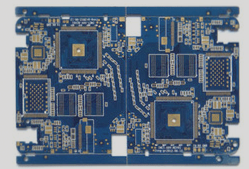
Here’s how your board should appear:

5. Compress All Files into a Single .zip File
The final step is to compress all the necessary files into one .zip file. Afterward, fill out the form with your PCB specifications (size, quantity, layers, thickness, etc.) on our “PCB Instant Quote” page and upload your .zip (Gerber) file. Our engineers will review it and provide feedback if there are any issues before fabrication.
Additional Resources:
If you have any questions about PCB or PCBA, feel free to contact us.