1. PCB board is the abbreviation for the English term “Printed Circuit Board.”
2. Typically, a conductive pattern, which can consist of printed circuits, printed components, or a combination of both, is designed on an insulating material.
3. This conductive pattern, which provides electrical connections between components on the insulating substrate, is known as a printed circuit.
4. Thus, a printed circuit or the completed board of the printed circuit is referred to as a printed circuit board, also known simply as a PCB.

1. The PCB board is integral to nearly all electronic devices, from electronic watches and calculators to computers, communication equipment, and military systems. Integrated circuits and other electronic components rely on PCBs for electrical interconnection, providing mechanical support, wiring, and insulation, as well as necessary electrical characteristics such as impedance. Additionally, PCBs feature solder mask graphics for automatic soldering and identification marks for component insertion, inspection, and maintenance.
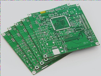
2. How are PCB boards made? When examining the health disk of a general-purpose computer, one might see a flexible insulating substrate with silver paste conductive and positioning graphics. This pattern, achieved through screen printing, defines the flexible silver paste printed circuit board. PCBs in computers, such as motherboards and graphics cards, use substrates made from paper base or glass cloth, with copper cladding laminated and cured on one or both sides. This results in a rigid board or a rigid printed circuit board. Boards with patterns on one side are single-sided, those with patterns on both sides are double-sided, and those with multiple layers are termed multilayer boards, which can exceed 100 layers.
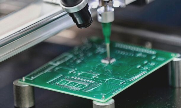
3. The PCB production process is intricate, involving various steps from simple to complex, including chemical reactions, photochemical, electrochemical, and thermochemical processes, as well as computer-aided design (CAM). Process issues frequently arise, and solving them can be challenging. Problems at any production stage can halt the entire line or lead to significant waste, increasing the pressure on process engineers and prompting many to transition to PCB equipment or material sales and services. To fully understand PCBs, it is essential to delve into the production processes of single-sided, double-sided, and multi-layer boards.
4. Single-sided rigid printed board: → single-sided copper clad laminate → blanking → (brushing, drying) → drilling or punching → screen printing anti-etching pattern or using dry film → curing, inspection, repair → etching copper → anti-corrosion removal, printing material, drying → brushing, drying → screen printing solder mask pattern (commonly green oil), UV curing → screen printing identification graphics, UV curing → preheating, punching, shaping → electrical open/short circuit test → brushing, drying → pre-coating with anti-oxidants or spraying with tin and hot air for leveling → inspection and packaging → finished product delivery.
5. Double-sided rigid printed board: → double-sided copper clad laminate → blanking → stacking → CNC drilling through holes → inspection, deburring, and brushing → chemical plating (through hole metallization) → (full board electroplating of thin copper) → inspection, brushing → screen printing negative circuit pattern, curing (dry or wet film, exposure, development) → inspection, repair → circuit pattern plating → electroplating tin (or nickel/gold) → printing material (photosensitive film) → etching copper → (tin stripping) → cleaning and brushing → screen printing solder mask pattern (heat-curing green oil, photosensitive dry or wet film) → cleaning, drying → screen printing identification graphics, curing → (spray tin or organic solder protection film) → shaping → cleaning, drying → electrical continuity testing → inspection and packaging → finished product delivery.
6. The process flow for through-hole metallization in multilayer boards builds on the double-sided process, with added steps for metallized hole inner layer interconnection, drilling, lamination, and special materials. Common computer boards use epoxy resin glass cloth-based double-sided PCBs, with one side for component insertion and the other for component foot welding. The regular appearance of solder joints on these pads is due to the solder mask that protects the board and prevents bridging during soldering. Most solder masks are green, but can also be yellow, black, or blue, and are referred to as green oil in the PCB industry. This mask protects the board from moisture, corrosion, mildew, and mechanical damage while ensuring high solder joint reliability.
7. Computer boards use three component installation methods: through-hole, surface mount, and direct chip mounting. Through-hole installation involves inserting components into PCB vias, which can be simple holes, double-sided interconnection vias, or positioning holes. Surface mount technology, including direct chip mounting, eliminates the need for through-holes, improving wiring density, reducing board area, and cutting design layers and costs. Surface mount also enhances product quality and reliability by reducing weight, improving shock resistance, and utilizing advanced soldering techniques.
2. Typically, a conductive pattern, which can consist of printed circuits, printed components, or a combination of both, is designed on an insulating material.
3. This conductive pattern, which provides electrical connections between components on the insulating substrate, is known as a printed circuit.
4. Thus, a printed circuit or the completed board of the printed circuit is referred to as a printed circuit board, also known simply as a PCB.

1. The PCB board is integral to nearly all electronic devices, from electronic watches and calculators to computers, communication equipment, and military systems. Integrated circuits and other electronic components rely on PCBs for electrical interconnection, providing mechanical support, wiring, and insulation, as well as necessary electrical characteristics such as impedance. Additionally, PCBs feature solder mask graphics for automatic soldering and identification marks for component insertion, inspection, and maintenance.
2. How are PCB boards made? When examining the health disk of a general-purpose computer, one might see a flexible insulating substrate with silver paste conductive and positioning graphics. This pattern, achieved through screen printing, defines the flexible silver paste printed circuit board. PCBs in computers, such as motherboards and graphics cards, use substrates made from paper base or glass cloth, with copper cladding laminated and cured on one or both sides. This results in a rigid board or a rigid printed circuit board. Boards with patterns on one side are single-sided, those with patterns on both sides are double-sided, and those with multiple layers are termed multilayer boards, which can exceed 100 layers.
3. The PCB production process is intricate, involving various steps from simple to complex, including chemical reactions, photochemical, electrochemical, and thermochemical processes, as well as computer-aided design (CAM). Process issues frequently arise, and solving them can be challenging. Problems at any production stage can halt the entire line or lead to significant waste, increasing the pressure on process engineers and prompting many to transition to PCB equipment or material sales and services. To fully understand PCBs, it is essential to delve into the production processes of single-sided, double-sided, and multi-layer boards.
4. Single-sided rigid printed board: → single-sided copper clad laminate → blanking → (brushing, drying) → drilling or punching → screen printing anti-etching pattern or using dry film → curing, inspection, repair → etching copper → anti-corrosion removal, printing material, drying → brushing, drying → screen printing solder mask pattern (commonly green oil), UV curing → screen printing identification graphics, UV curing → preheating, punching, shaping → electrical open/short circuit test → brushing, drying → pre-coating with anti-oxidants or spraying with tin and hot air for leveling → inspection and packaging → finished product delivery.
5. Double-sided rigid printed board: → double-sided copper clad laminate → blanking → stacking → CNC drilling through holes → inspection, deburring, and brushing → chemical plating (through hole metallization) → (full board electroplating of thin copper) → inspection, brushing → screen printing negative circuit pattern, curing (dry or wet film, exposure, development) → inspection, repair → circuit pattern plating → electroplating tin (or nickel/gold) → printing material (photosensitive film) → etching copper → (tin stripping) → cleaning and brushing → screen printing solder mask pattern (heat-curing green oil, photosensitive dry or wet film) → cleaning, drying → screen printing identification graphics, curing → (spray tin or organic solder protection film) → shaping → cleaning, drying → electrical continuity testing → inspection and packaging → finished product delivery.
6. The process flow for through-hole metallization in multilayer boards builds on the double-sided process, with added steps for metallized hole inner layer interconnection, drilling, lamination, and special materials. Common computer boards use epoxy resin glass cloth-based double-sided PCBs, with one side for component insertion and the other for component foot welding. The regular appearance of solder joints on these pads is due to the solder mask that protects the board and prevents bridging during soldering. Most solder masks are green, but can also be yellow, black, or blue, and are referred to as green oil in the PCB industry. This mask protects the board from moisture, corrosion, mildew, and mechanical damage while ensuring high solder joint reliability.
7. Computer boards use three component installation methods: through-hole, surface mount, and direct chip mounting. Through-hole installation involves inserting components into PCB vias, which can be simple holes, double-sided interconnection vias, or positioning holes. Surface mount technology, including direct chip mounting, eliminates the need for through-holes, improving wiring density, reducing board area, and cutting design layers and costs. Surface mount also enhances product quality and reliability by reducing weight, improving shock resistance, and utilizing advanced soldering techniques.


