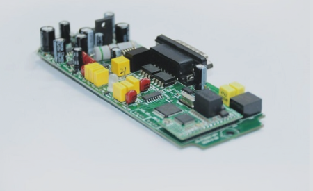
SMT Patch Processing in PCBA Plants
Preparation Work for Efficient Production
- Thorough pre-production preparations are crucial for smooth SMT patch processing in PCBA plants.
- Standardized production process management is essential for timely completion.
- Engineering tasks include planned order arrangements, material checks, and sample completion.
Production Steps
- SMT Patch Processing:
- Confirm material readiness and tools 2 hours before production.
- Coordinate for supplementary materials if needed.
- Inspect pieces for defects and address issues promptly.
- DIP Plug-In Processing:
- Schedule material preparation and confirm quality.
- Determine auxiliary materials in advance.
- Conduct pre-production meetings for each product.
Quality Assurance
- IPQC inspections and quality confirmations are critical for both SMT and DIP processes.
- Adherence to planned orders and timely quality checks are emphasized.
Process Optimization
- Streamlined production and testing processes for new and return orders.
- Integration of SMT and DIP processes for efficient assembly.
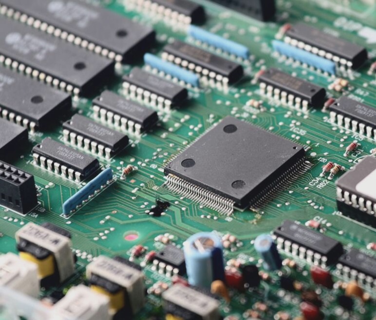
Key Elements in SMT Patch Processing
SMT patch processing involves essential steps in PCB technology:
- Silk Screen (Glue Dispensing): Application of solder paste or glue on PCB pads.
- Dispensing: Fixing components onto the PCB using specialized equipment.
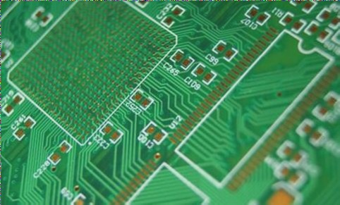
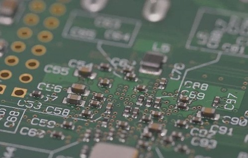
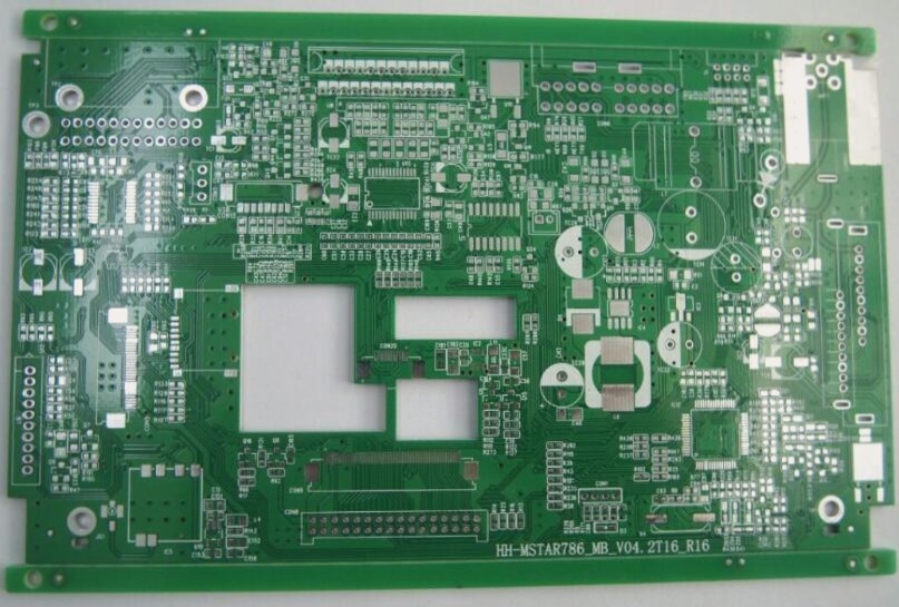
PCB Manufacturing Process Steps:
- 1. **Design:** The initial stage involves creating a layout design for the PCB, determining component placement and connection routes.
- 2. **Printing (Etching):** This step uses a chemical process to remove excess copper from the PCB, leaving behind the desired circuit pattern.
- 3. **Placement (Curing):** To ensure precise installation of surface-mount components, a placement machine is utilized after the printing process.
- 4. **Reflow Soldering:** By utilizing a reflow oven, the solder paste is melted to securely bond the surface-mounted components onto the PCB.
- 5. **Cleaning:** The final step involves eliminating any harmful solder residue from the assembled PCB, using a cleaning machine placed strategically as required.