PCB Lamination Process Overview
Before lamination, the inner image layer surface must undergo an oxidation process to roughen and passivate the copper surface. This enhances resin interaction, improving bond strength between copper and prepreg, preventing issues like delamination and diffusion coating.
Lay-up Process
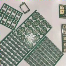
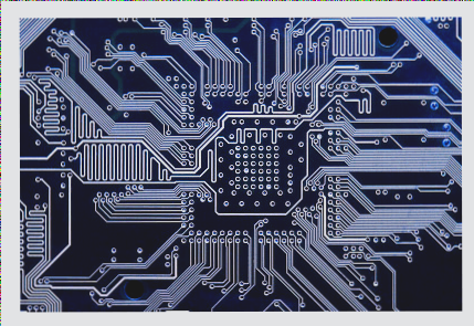
For multi-layer boards, a preliminary lay-up stacks core boards, etched circuit patterns, and prepreg in a specific order. Inner layers are fixed to prevent misalignment, ensuring aligned traces and avoiding potential open or short circuits. The lay-up involves stacking materials in the correct order for lamination.
Lamination Steps
Inner layers, clamped between iron plates, are placed onto stands and fed into a vacuum heat press machine. High temperature and pressure melt the resin in the prepreg, bonding the layers together. After lamination, operators remove the top iron plate and supporting aluminum plate. This step is necessary for boards with three or more layers.
Post-Treatment
After lamination, boards undergo bevelling, target drilling, edge milling, and other treatments. Layer deviation checking via X-ray inspection and hole milling are crucial processes in post-treatment.
If you have any questions about PCBs and PCBA, please contact us at info@wellcircuits.com.


