Portable Multifunctional Electronic Products and PCB Demands
High Demands on PCBs for Electronic Products
- Portable electronic products require close interconnection of components in limited spaces.
- Circuit stabilization is crucial for optimal performance.
Increasing Density of Circuit Boards
- Boards are becoming denser with reduced sizes of openings and line widths.
- Improvements in distances and precision between components.
- Aspect ratio of vias is increasing.
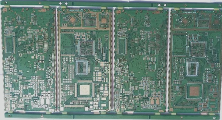
Challenges in PCB Manufacturing
- Over 10 circuit layers with more than 50,000 microvias in a single layer.
- Microvias spacing as small as 0.05 mm with diameters less than 150 μm.
- Challenges in mechanically drilling boards due to material, cooling, and accuracy issues.
Laser Processing for Quality Improvement
Utilizing laser processing is more effective in meeting stringent quality requirements for PCB manufacturing.
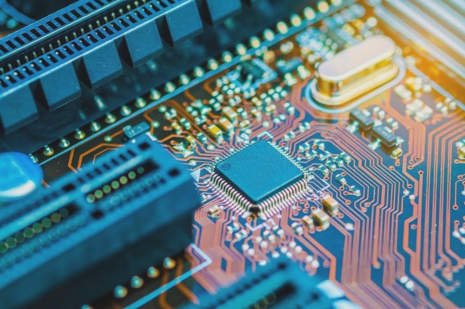
Application of Laser Beam
The high-density PCBs from WellCircuits feature a multi-layer structure with copper foil and insulating resin. Laser processing involves melting and vaporizing materials to create small holes, with careful control of parameters such as beam wavelength and mode.
Influence of Beam Wavelength and Mode on Machining
Selection of laser wavelength and mode affects the drilling process, with different lasers suitable for various types of PCBs. Carbon dioxide lasers are ideal for high-density boards due to their high absorption rates for copper foil.
Influence of Beam Pulse
Using multi-pulse lasers requires controlling the output density to ensure effective drilling without damaging the substrate. Optimal energy levels are crucial for creating tapered hole patterns beneficial for subsequent processes.
Laser Beam Effect
The interaction between the laser beam and PCB materials influences micropores’ characteristics, aperture, and depth.
The Interaction Between Laser and PCB
When a laser interacts with a PCB, it first encounters the copper foil on the surface. Copper foil has a low absorption rate for infrared wavelength carbon dioxide lasers, making efficient processing challenging. The absorbed light energy increases the kinetic energy of free electrons in the copper foil, mostly converting into heat. Enhancing light absorption on the copper foil surface by coating it with a material can improve the laser absorption rate.
Effect of Beam Impact
During laser processing, the light heats and vaporizes the copper foil material, leading to the formation of high-temperature steam, which can decompose and ionize, creating photo-induced plasma. This plasma can either enhance or block laser energy absorption by the workpiece, depending on its energy delivery. To control plasma effects, maintaining laser power density below 10^7 W/cm² is crucial. The pinhole effect plays a significant role in increasing light energy absorption during laser drilling, ensuring the desired depth and hole size.
Conclusion
Laser processing technology significantly improves the drilling efficiency of high-density PCB micro-holes. Experiments show that combining numerical control technology enables processing over 30,000 micro-holes per minute on PCBs with diameters from 75 to 100 μm. Additionally, using ultraviolet lasers can further reduce hole sizes below 50 μm, expanding the usable area of PCB boards.