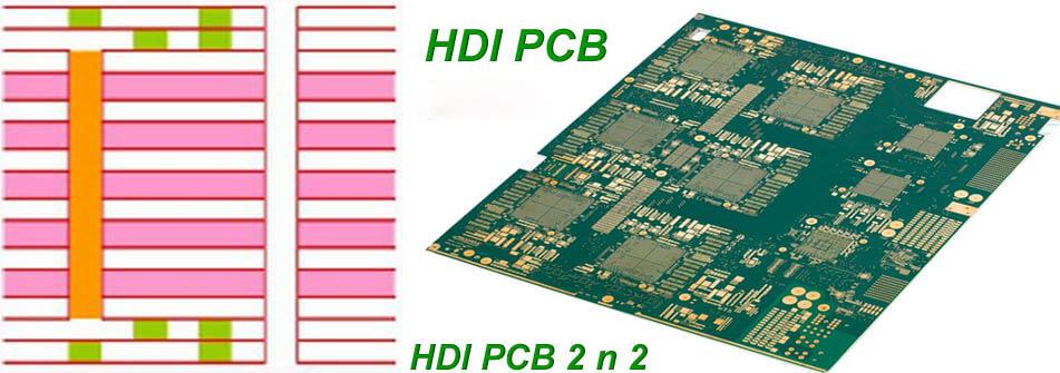
1. With the rapid development of micro-electronics technology, the extensive use of large-scale and ultra-large-scale integrated circuits, and advancements in micro-assembly technology, HDI PCB circuit board manufacturing is evolving toward a layered and multifunctional approach. Consequently, the graphic traces on PCB circuit boards are becoming thinner and more micro-porous with narrower spacing. Traditional mechanical drilling methods are no longer sufficient to meet these requirements, leading to the rapid development of new micro-hole processing techniques, such as laser drilling technology.
2. **Principle of Laser Hole Formation for HDI PCB**
3. Laser is a concentrated beam of light stimulated by an external source to increase its energy. Infrared and visible light possess thermal energy, while ultraviolet light contains optical energy. When this light interacts with the surface of a workpiece, three phenomena can occur: reflection, absorption, and penetration.
4. A laser spot can be directed onto a substrate through various optical methods, resulting in multiple compositional modes and three distinct reactions at the illuminated point.
5. The primary function of laser drilling is to efficiently remove substrate material. This process relies mainly on photothermal ablation and photochemical ablation, also known as excision.
6. **Photothermal ablation:** This process involves a material absorbing high-energy laser light, which heats the material to the point of melting and evaporation in a very short time. High energy leads to the formation of black charred residue on the pore wall, which must be cleaned before further processing.
7. **Photochemical ablation:** This process occurs when high-energy photons in the ultraviolet region, with energies exceeding 2eV, interact with the material. High-energy photons with laser wavelengths over 400 nanometers break down the long molecular chains in organic materials into smaller particles. These smaller particles, having higher energy than the original molecules, escape, resulting in rapid material removal and the formation of micro-pores under external conditions.
8. Therefore, this process does not involve boiling or carbonization, making pre-porosization cleaning relatively straightforward.
9. These are the fundamental principles of laser pore formation. Currently, two primary laser drilling methods are commonly used: RF-excited CO2 gas lasers and UV solid-state Nd:YAG lasers.
10. **About the absorbance of the base plate:** The effectiveness of laser drilling is directly related to the absorbance of the base material. A printed circuit board is composed of copper foil, glass cloth, and resin. The absorbance of these materials varies with wavelength. Copper foil and glass cloth have higher absorbance in ultraviolet light, typically below 0.3 μm, but their absorbance drops sharply in visible light and infrared. Organic resin materials, on the other hand, maintain relatively high absorbance across all three spectral regions. This characteristic of resin materials is a key factor in the widespread adoption of laser drilling technology.

Here are the revised sections:
**Different HDI PCB Processes for CO2 Laser Hole Formation**
There are two primary methods for CO2 laser drilling: direct drilling and mask dressing drilling. Direct hole-forming technology involves adjusting the laser beam diameter to match the hole diameter on the printed circuit board, allowing for direct processing on the dielectric surface without copper foil. The mask dressing process involves applying a special mask to the surface of the printed board, then using conventional techniques to remove the copper foil from the hole surface. Afterward, a larger laser beam irradiates the exposed dielectric layer resin to remove it. These methods are detailed as follows:
1. **Bronze Window Opening Method:**
First, press a layer of RCC-coated resin copper foil onto the inner panel. Create a window using photochemistry, then etch the resin to expose it. The substrate material inside the window is ablated by laser to form a micro-blind hole. As the beam is enhanced, it passes through the aperture to reach two groups of galvanometer-type micro-reflective scanners, which are aligned vertically with the positive F θ Lens. The micro-blind holes are then burned one by one. Positioned by an electron fast beam within an inch-square tubular area, a 0.15mm blind hole can be punched with three shots. The first shot has a pulse width of about 15 μs, which provides the energy needed for hole formation. Subsequent shots clean the residue at the bottom of the hole and correct the hole. SEM cross-sections and 45-degree full views of the 0.15mm micro-blind hole, with effective laser energy control, demonstrate this process. The window-opening method is used as a backing target plate. Large typesetting or second-order blind holes are less frequent, making alignment challenging.
2. **Opening Window Process Method:**
The diameter of holes formed by this process matches that of the open copper window. Slight operational errors may cause misalignment between the open window and the center of the base pad. Copper window deviations can result from matrix material expansion and contraction or distortion of the negative used for image transfer. To address this, the process involves enlarging the diameter of the copper window by 0.05mm compared to the base pad. For a 0.15mm hole, the base pad diameter should be about 0.25mm, and the large window should be 0.30mm. Laser drilling can then precisely align the burnout position with the micro-blind hole of the base pad. This approach allows flexibility in hole drilling, minimizing misalignment caused by matching the copper window diameter to the hole diameter, which can lead to incomplete holes or residual holes in large batches.
3. **Direct Pore Forming Process on HDI PCB Resin Surface:**
Several methods are used for laser drilling on HDI PCB surfaces:
A. Resin-coated copper foil is pressed onto the base plate’s inner layer, then etched off. CO2 laser can then directly form holes on the bare resin surface, followed by further treatment as per the plating process.
B. An alternative involves using FR-4 semi-cured sheets and copper foil instead of resin-coated copper foil.
C. A process for subsequent lamination of copper foil with coated photosensitive resin.
D. Dry film is used as a dielectric layer, followed by copper foil pressing.
E. Other types of warm film with copper foil coating.
4. **Direct Ablation of Ultra-Thin Copper Foil:**
After pressing resin copper foil on both sides of the inner core plate, reduce the copper foil thickness from 17μm to 5μm using the “half etching” method. Black oxidation is then applied, allowing holes to be formed by CO2 laser. The principle is that the oxidized black surface absorbs light intensively, enabling direct ablation of the ultra-thin copper foil and resin surface by increasing the CO2 laser beam energy. Ensuring uniform thickness with the “half etching” method is crucial, as is using copper-backed tearable material UTC, which is approximately 5μm thick. The process must maintain strict quality and technical criteria for material suppliers to ensure dielectric layer thickness uniformity of 510 μm to 1mm. Proper laser energy and cleanliness of the hole bottom are vital for high-quality electroless and electroplating.
**Nd:YAG Laser Drilling HDI PCB Process:**
Nd:YAG laser uses neodymium and yttrium aluminium garnet crystals to emit UV laser. Recently, diode-pulsed lasers have been utilized for effective sealing without water cooling. The third-harmonic wavelength is 355 nanometers, and the fourth-harmonic wavelength is 266 nanometers. This laser is noted for its UV spectrum region, where copper foil and glass fibers in copper-clad laminates strongly absorb UV light. This enables the laser to penetrate the copper foil and glass cloth to form holes directly. The low laser heat minimizes charcoal slag, providing a clean surface for subsequent operations. Nd:YAG lasers can process logo blind holes and pass-through holes with a minimum diameter of 25 microns, with a most economical diameter of 25-125 microns, at speeds of up to 10,000 holes/min. It can also drill PTFE copper-clad laminates with a minimum diameter of 25 microns and a most economical diameter of 25-125 microns, at speeds of 4,500 holes/min. No pre-etching is required, and the holes are clean without special processing needs. Two combined processes are used: YAG lasers to ablate the copper foil, followed by faster CO2 lasers to ablate the resin and form the hole.
**Quality Problems in Actual HDI PCB Manufacturing:**
Several quality issues arise in laser drilling. Common problems include:
A. **Misalignment between CO2 Laser Drilling Position and Bottom Target Position in Open-Window Method:**
Accurate beam positioning is crucial for aperture shaping. Common issues include:
1. Size changes in the negative for the inner core plate or window opening due to humidity and temperature.
2. Dimension changes in the base material and resin-coated copper foil during high-temperature pressing and layer addition.
3. Errors from the size and position of the etched copper window.
4. Laser light point errors and surface displacement.
5. Difficulties in aligning second-order blind holes.
Technological strategies to address these issues include:
1. Reducing typesetting size, with optimal sizes for mobile phone panels.
2. Increasing laser diameter to cover more copper window area and compensating for low energy density.
3. Enlarging the copper window while maintaining hole diameter to avoid misalignment.
4. Switching from photochemical imaging to YAG laser for opening windows to reduce imaging errors.
5. Using a second-order micro-blind hole method with precise alignment targeting.
B. **Incorrect Pass:**
Quality issues often stem from base material shaping and dielectric layer thickness variations. Variations can cause uneven energy distribution during drilling, leading to outward-expanding hole walls. This impacts multilayer interconnect reliability. Solutions include:
1. Strictly controlling dielectric layer thickness differences.
2. Adjusting laser energy density and pulse number based on test results.
3. Ensuring proper removal of slag and debris from hole walls.
Quality problems in large plates with numerous micro-blind holes are challenging to avoid entirely, especially with varying media layer thicknesses. Accurate inspection and treatment are essential to prevent defects in copper plating and bond quality.
2. **Principle of Laser Hole Formation for HDI PCB**
3. Laser is a concentrated beam of light stimulated by an external source to increase its energy. Infrared and visible light possess thermal energy, while ultraviolet light contains optical energy. When this light interacts with the surface of a workpiece, three phenomena can occur: reflection, absorption, and penetration.
4. A laser spot can be directed onto a substrate through various optical methods, resulting in multiple compositional modes and three distinct reactions at the illuminated point.
5. The primary function of laser drilling is to efficiently remove substrate material. This process relies mainly on photothermal ablation and photochemical ablation, also known as excision.
6. **Photothermal ablation:** This process involves a material absorbing high-energy laser light, which heats the material to the point of melting and evaporation in a very short time. High energy leads to the formation of black charred residue on the pore wall, which must be cleaned before further processing.
7. **Photochemical ablation:** This process occurs when high-energy photons in the ultraviolet region, with energies exceeding 2eV, interact with the material. High-energy photons with laser wavelengths over 400 nanometers break down the long molecular chains in organic materials into smaller particles. These smaller particles, having higher energy than the original molecules, escape, resulting in rapid material removal and the formation of micro-pores under external conditions.
8. Therefore, this process does not involve boiling or carbonization, making pre-porosization cleaning relatively straightforward.
9. These are the fundamental principles of laser pore formation. Currently, two primary laser drilling methods are commonly used: RF-excited CO2 gas lasers and UV solid-state Nd:YAG lasers.
10. **About the absorbance of the base plate:** The effectiveness of laser drilling is directly related to the absorbance of the base material. A printed circuit board is composed of copper foil, glass cloth, and resin. The absorbance of these materials varies with wavelength. Copper foil and glass cloth have higher absorbance in ultraviolet light, typically below 0.3 μm, but their absorbance drops sharply in visible light and infrared. Organic resin materials, on the other hand, maintain relatively high absorbance across all three spectral regions. This characteristic of resin materials is a key factor in the widespread adoption of laser drilling technology.

Here are the revised sections:
**Different HDI PCB Processes for CO2 Laser Hole Formation**
There are two primary methods for CO2 laser drilling: direct drilling and mask dressing drilling. Direct hole-forming technology involves adjusting the laser beam diameter to match the hole diameter on the printed circuit board, allowing for direct processing on the dielectric surface without copper foil. The mask dressing process involves applying a special mask to the surface of the printed board, then using conventional techniques to remove the copper foil from the hole surface. Afterward, a larger laser beam irradiates the exposed dielectric layer resin to remove it. These methods are detailed as follows:
1. **Bronze Window Opening Method:**
First, press a layer of RCC-coated resin copper foil onto the inner panel. Create a window using photochemistry, then etch the resin to expose it. The substrate material inside the window is ablated by laser to form a micro-blind hole. As the beam is enhanced, it passes through the aperture to reach two groups of galvanometer-type micro-reflective scanners, which are aligned vertically with the positive F θ Lens. The micro-blind holes are then burned one by one. Positioned by an electron fast beam within an inch-square tubular area, a 0.15mm blind hole can be punched with three shots. The first shot has a pulse width of about 15 μs, which provides the energy needed for hole formation. Subsequent shots clean the residue at the bottom of the hole and correct the hole. SEM cross-sections and 45-degree full views of the 0.15mm micro-blind hole, with effective laser energy control, demonstrate this process. The window-opening method is used as a backing target plate. Large typesetting or second-order blind holes are less frequent, making alignment challenging.
2. **Opening Window Process Method:**
The diameter of holes formed by this process matches that of the open copper window. Slight operational errors may cause misalignment between the open window and the center of the base pad. Copper window deviations can result from matrix material expansion and contraction or distortion of the negative used for image transfer. To address this, the process involves enlarging the diameter of the copper window by 0.05mm compared to the base pad. For a 0.15mm hole, the base pad diameter should be about 0.25mm, and the large window should be 0.30mm. Laser drilling can then precisely align the burnout position with the micro-blind hole of the base pad. This approach allows flexibility in hole drilling, minimizing misalignment caused by matching the copper window diameter to the hole diameter, which can lead to incomplete holes or residual holes in large batches.
3. **Direct Pore Forming Process on HDI PCB Resin Surface:**
Several methods are used for laser drilling on HDI PCB surfaces:
A. Resin-coated copper foil is pressed onto the base plate’s inner layer, then etched off. CO2 laser can then directly form holes on the bare resin surface, followed by further treatment as per the plating process.
B. An alternative involves using FR-4 semi-cured sheets and copper foil instead of resin-coated copper foil.
C. A process for subsequent lamination of copper foil with coated photosensitive resin.
D. Dry film is used as a dielectric layer, followed by copper foil pressing.
E. Other types of warm film with copper foil coating.
4. **Direct Ablation of Ultra-Thin Copper Foil:**
After pressing resin copper foil on both sides of the inner core plate, reduce the copper foil thickness from 17μm to 5μm using the “half etching” method. Black oxidation is then applied, allowing holes to be formed by CO2 laser. The principle is that the oxidized black surface absorbs light intensively, enabling direct ablation of the ultra-thin copper foil and resin surface by increasing the CO2 laser beam energy. Ensuring uniform thickness with the “half etching” method is crucial, as is using copper-backed tearable material UTC, which is approximately 5μm thick. The process must maintain strict quality and technical criteria for material suppliers to ensure dielectric layer thickness uniformity of 510 μm to 1mm. Proper laser energy and cleanliness of the hole bottom are vital for high-quality electroless and electroplating.
**Nd:YAG Laser Drilling HDI PCB Process:**
Nd:YAG laser uses neodymium and yttrium aluminium garnet crystals to emit UV laser. Recently, diode-pulsed lasers have been utilized for effective sealing without water cooling. The third-harmonic wavelength is 355 nanometers, and the fourth-harmonic wavelength is 266 nanometers. This laser is noted for its UV spectrum region, where copper foil and glass fibers in copper-clad laminates strongly absorb UV light. This enables the laser to penetrate the copper foil and glass cloth to form holes directly. The low laser heat minimizes charcoal slag, providing a clean surface for subsequent operations. Nd:YAG lasers can process logo blind holes and pass-through holes with a minimum diameter of 25 microns, with a most economical diameter of 25-125 microns, at speeds of up to 10,000 holes/min. It can also drill PTFE copper-clad laminates with a minimum diameter of 25 microns and a most economical diameter of 25-125 microns, at speeds of 4,500 holes/min. No pre-etching is required, and the holes are clean without special processing needs. Two combined processes are used: YAG lasers to ablate the copper foil, followed by faster CO2 lasers to ablate the resin and form the hole.
**Quality Problems in Actual HDI PCB Manufacturing:**
Several quality issues arise in laser drilling. Common problems include:
A. **Misalignment between CO2 Laser Drilling Position and Bottom Target Position in Open-Window Method:**
Accurate beam positioning is crucial for aperture shaping. Common issues include:
1. Size changes in the negative for the inner core plate or window opening due to humidity and temperature.
2. Dimension changes in the base material and resin-coated copper foil during high-temperature pressing and layer addition.
3. Errors from the size and position of the etched copper window.
4. Laser light point errors and surface displacement.
5. Difficulties in aligning second-order blind holes.
Technological strategies to address these issues include:
1. Reducing typesetting size, with optimal sizes for mobile phone panels.
2. Increasing laser diameter to cover more copper window area and compensating for low energy density.
3. Enlarging the copper window while maintaining hole diameter to avoid misalignment.
4. Switching from photochemical imaging to YAG laser for opening windows to reduce imaging errors.
5. Using a second-order micro-blind hole method with precise alignment targeting.
B. **Incorrect Pass:**
Quality issues often stem from base material shaping and dielectric layer thickness variations. Variations can cause uneven energy distribution during drilling, leading to outward-expanding hole walls. This impacts multilayer interconnect reliability. Solutions include:
1. Strictly controlling dielectric layer thickness differences.
2. Adjusting laser energy density and pulse number based on test results.
3. Ensuring proper removal of slag and debris from hole walls.
Quality problems in large plates with numerous micro-blind holes are challenging to avoid entirely, especially with varying media layer thicknesses. Accurate inspection and treatment are essential to prevent defects in copper plating and bond quality.


