1. FPC circuit boards can be classified into single-sided, double-sided, and multi-layer boards based on the number of circuit layers. Common multi-layer boards typically have 4 or 6 layers, but complex multi-layer boards can have dozens of layers.
2. There are three main types of circuit boards:
3. **Single-Sided Boards**
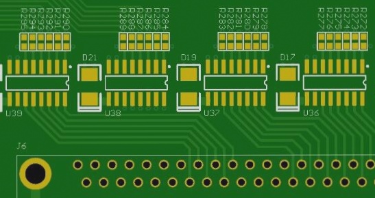
Single-sided boards are the most basic type of PCB, with components concentrated on one side and the wiring on the other. For boards with SMD components, both the components and the wiring are on the same side, while through-hole components are placed on the opposite side. Since the wiring appears on only one side, these PCBs are referred to as single-sided. This type of board imposes significant design restrictions due to the necessity of routing wires without crossing them, limiting its use mainly to simpler, early circuit designs.
4. **Double-Sided Boards**

### Double-Sided Boards
1. **Double-sided boards** have wiring on both sides, but to utilize both sides, there must be a proper circuit connection between them. The “bridges” connecting these circuits are called vias. A via is a small hole filled or coated with metal on the PCB, enabling connections between the wires on both sides.
2. Because the area of a double-sided board is twice that of a single-sided board, it addresses the challenges of interlaced wiring found in single-sided boards by allowing connections through the holes. This makes it more suitable for circuits that are more complex than those typically handled by single-sided boards.
### Multilayer Boards
3. **Multilayer boards** increase the wiring area by stacking multiple single-sided or double-sided boards. Typically, one double-sided board serves as the inner layer, with two single-sided boards as the outer layers, or two double-sided boards as the inner layers with two single-sided boards as the outer layers.
4. The boards are assembled with insulating bonding material and conductive patterns according to design specifications, resulting in four-layer or six-layer printed circuit boards, also known as multilayer printed circuit boards. The number of layers does not necessarily indicate separate wiring layers; sometimes, empty layers are added to control board thickness.
5. Most motherboards feature a structure of 4 to 8 layers, but technically, boards can have nearly 100 layers. While supercomputers often use highly multilayered boards, they are increasingly replaced by clusters of standard computers, reducing the use of super-multilayered boards. The tightly integrated layers of a PCB make it difficult to discern the exact number, but a close examination of the motherboard can reveal it.
### Features
6. **PCB** technology is widely used due to several unique advantages:
7. **High Density:** Over decades, the high density of printed boards has evolved with advancements in integrated circuit integration and mounting technology.
8. **High Reliability:** Through rigorous inspections, tests, and aging processes, PCBs can operate reliably for extended periods, typically around 20 years.
9. **Design Flexibility:** PCBs can be designed to meet various performance requirements (electrical, physical, chemical, mechanical) through standardization and efficient design practices.
10. **Producibility:** Modern management enables standardized, scaled, and automated production, ensuring consistent product quality.
11. **Testability:** Established testing methods, standards, and equipment help in detecting and evaluating PCB product quality and longevity.
12. **Assemblability:** PCBs facilitate standardized, automated, and large-scale assembly of various components, allowing for the creation of larger parts and systems, up to complete machines.
13. **Maintainability:** Standardization in design and production means that parts can be quickly, conveniently, and flexibly replaced, enabling rapid system restoration. This includes benefits like system miniaturization, weight reduction, and high-speed signal transmission.
2. There are three main types of circuit boards:
3. **Single-Sided Boards**
Single-sided boards are the most basic type of PCB, with components concentrated on one side and the wiring on the other. For boards with SMD components, both the components and the wiring are on the same side, while through-hole components are placed on the opposite side. Since the wiring appears on only one side, these PCBs are referred to as single-sided. This type of board imposes significant design restrictions due to the necessity of routing wires without crossing them, limiting its use mainly to simpler, early circuit designs.
4. **Double-Sided Boards**

### Double-Sided Boards
1. **Double-sided boards** have wiring on both sides, but to utilize both sides, there must be a proper circuit connection between them. The “bridges” connecting these circuits are called vias. A via is a small hole filled or coated with metal on the PCB, enabling connections between the wires on both sides.
2. Because the area of a double-sided board is twice that of a single-sided board, it addresses the challenges of interlaced wiring found in single-sided boards by allowing connections through the holes. This makes it more suitable for circuits that are more complex than those typically handled by single-sided boards.
### Multilayer Boards
3. **Multilayer boards** increase the wiring area by stacking multiple single-sided or double-sided boards. Typically, one double-sided board serves as the inner layer, with two single-sided boards as the outer layers, or two double-sided boards as the inner layers with two single-sided boards as the outer layers.
4. The boards are assembled with insulating bonding material and conductive patterns according to design specifications, resulting in four-layer or six-layer printed circuit boards, also known as multilayer printed circuit boards. The number of layers does not necessarily indicate separate wiring layers; sometimes, empty layers are added to control board thickness.
5. Most motherboards feature a structure of 4 to 8 layers, but technically, boards can have nearly 100 layers. While supercomputers often use highly multilayered boards, they are increasingly replaced by clusters of standard computers, reducing the use of super-multilayered boards. The tightly integrated layers of a PCB make it difficult to discern the exact number, but a close examination of the motherboard can reveal it.
### Features
6. **PCB** technology is widely used due to several unique advantages:
7. **High Density:** Over decades, the high density of printed boards has evolved with advancements in integrated circuit integration and mounting technology.
8. **High Reliability:** Through rigorous inspections, tests, and aging processes, PCBs can operate reliably for extended periods, typically around 20 years.
9. **Design Flexibility:** PCBs can be designed to meet various performance requirements (electrical, physical, chemical, mechanical) through standardization and efficient design practices.
10. **Producibility:** Modern management enables standardized, scaled, and automated production, ensuring consistent product quality.
11. **Testability:** Established testing methods, standards, and equipment help in detecting and evaluating PCB product quality and longevity.
12. **Assemblability:** PCBs facilitate standardized, automated, and large-scale assembly of various components, allowing for the creation of larger parts and systems, up to complete machines.
13. **Maintainability:** Standardization in design and production means that parts can be quickly, conveniently, and flexibly replaced, enabling rapid system restoration. This includes benefits like system miniaturization, weight reduction, and high-speed signal transmission.


