6-Layer PCB Fabrication Process
A 6-layer PCB, also known as a “multi-layer board,” consists of three copper-clad laminates. The fabrication process involves cutting the metal sheet and sequentially pressing the inner layers with drilled holes. After the initial pressing, the board undergoes a second pressing and subsequent drilling, followed by processes like copper electroplating for further production.
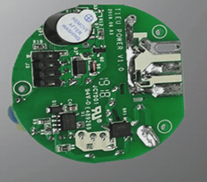
These printed circuit boards are commonly utilized in the communications industry due to their versatility and performance capabilities.

Thickness Considerations for 6-Layer PCBs
The 6-layer PCB can accommodate various thickness requirements, with 1.6mm being the most common option. During the pressing process, the substrate’s resin melts and redistributes under high temperatures, resulting in an overall thickness of 1.6mm.
Numerical calculations for a 6-layer board include core board thickness, PP thickness, and pressed copper foil thickness, with the total sum averaging around 1.63mm.
Varying Thickness Based on Application
- For power boards, thicker copper layers are preferred for enhanced operational reliability.
- Standard precision products typically follow standard copper foil requirements.