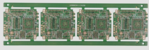
Sequential Lamination Method for Buried/Blind Vias in PCB Manufacturing
Advancements in electronic housing technology have led to the emergence of flexible boards, rigid-flex boards, and buried/blind-hole multilayer PCBs. To meet the demands for smaller, lighter, and thinner electronic products, manufacturers are adopting the sequential lamination method for PCB production.
Challenges and Solutions:
- CAD Wiring: When using the sequential lamination method, it is crucial to consider the technological limitations. To simplify the process, prioritize the use of buried vias over blind vias and limit the number of interconnections.
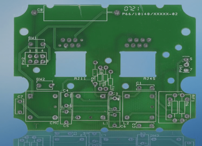
- Inner Layer Production: Proper identification and differentiation of metallized and non-metallized holes in inner layers are essential. Inner layer drilling programs should align with core board labels to ensure accuracy.
- Lamination: Attention to detail during lamination is key. Verify the correct lamination sequence, alignment of inner layers, and resin fill in prepreg holes. Selecting the right semi-cured prepreg type and copper foil thickness is critical for successful lamination.
- Outer Layer Graphic Production: Due to varying copper foil thickness caused by blind holes, adjustments in the etching process are necessary. Consider compensating for these differences during photomask drawing to prevent warping in the final product.
Latest Updates:
In recent developments, manufacturers are exploring advanced laser drilling machines and pulse plating equipment to enhance the production of buried/blind-via multilayer PCBs. By investing in cutting-edge technology, companies can offer a wider range of products to meet diverse customer needs.