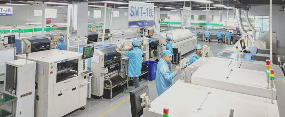
SMT Chip Processing Component Layout Design
Key Considerations for Component Layout Design in SMT Chip Processing
- Component Distribution: Ensure uniform distribution of components on the PCB to prevent issues like virtual soldering due to excessive concentration of large-mass components during reflow soldering.
- Arrangement Direction: Arrange similar components in the same direction for ease of mounting, welding, and testing. Consistent orientation of part numbers is crucial.
- Equipment Operation: Leave adequate space around large components to accommodate the size of SMD rework equipment heating heads for effective operation.
- Isolation of Heat-Generating Components: Position heat-generating components away from other parts, preferably in ventilated corners within the chassis.
- Thermal Dissipation: Support heating components with leads, heat sinks, or other supports to maintain a minimum distance of 2mm from the PCB surface. Connect heating elements to metal pads for heat dissipation.
- Protection of Temperature-Sensitive Components: Keep temperature-sensitive components like triodes and integrated circuits away from heat sources such as high-power resistors to prevent damage.
It is essential to tailor the component layout design to the specific production equipment and process characteristics of SMT chip processing. Different processes like reflow soldering and wave soldering have unique requirements that must be considered for optimal performance.
For instance, during double-sided reflow soldering, distinct layout requirements exist for each side, and selective wave soldering differs from traditional wave soldering in terms of component layout. By adhering to the fundamental requirements outlined above, manufacturers can ensure efficient and reliable SMT processes.

