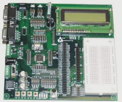
1. The heat dissipation of a PCB board is an essential aspect to consider. Untimely heat dissipation can result in component burnout, excessive energy consumption, and a shortened lifespan of the PCB board. Therefore, when designing a PCB, technicians must take into account various factors, including the heat transfer generated by components.
2. After years of discussion and research, it has been concluded that the most effective way to address heat dissipation is to enhance the heat dissipation capacity of the PCB board that comes into direct contact with the heating components, and to transmit or distribute heat through the PCB board.
PCB board heat dissipation layout
1) The thermal sensor should be placed in the coolest area.
2) The temperature detector should be placed at the hottest position on the PCB board.
3) Components on the same PCB board should be arranged in zones according to their calorific value and heat dissipation degree. Components with low calorific value or poor heat resistance (such as small signal transistors, small-scale integrated circuits, electrolytic capacitors, etc.) should be placed at the top (entrance) of the cooling air flow, while components with high calorific value or good heat resistance (such as power transistors, large-scale integrated circuits, etc.) should be placed at the bottom of the cooling air flow.
4) In the horizontal direction, high-power devices should be arranged as close to the edge of the printed board as possible to shorten the heat transfer path. In the vertical direction, high-power devices should be arranged as close as possible to the top of the printed circuit board to reduce the impact on the temperature of other devices during operation.
5) The heat dissipation of the printed circuit board in the equipment mainly depends on the air flow, so the air flow path should be studied during the design, and the device or printed circuit board should be reasonably configured. When air flows, it always tends to flow in a place with small resistance. Therefore, when configuring components on the PCB board, it is necessary to avoid leaving a large space in a certain area. The configuration of multiple printed circuit boards in the whole machine should also pay attention to the same problem.
6) Devices that are sensitive to temperature should be placed in the area with the lowest temperature (such as the bottom of the equipment) and should not be placed directly above heating devices. Multiple devices should be staggered on the horizontal plane.
7) Devices with the highest power consumption and heat generation should be arranged near the best heat dissipation position. Components with high heat generation should not be placed on the corners and surrounding edges of the printed board, unless there is a heat sink near it. In the design of power resistance, a larger device should be selected as far as possible, and it should have enough heat dissipation space when adjusting the layout of the printed circuit board.
Conformal coating is vital for PCB boards, especially for those that must function in harsh environments. The PCB protective coating can protect the circuit board from corrosion, moisture, and dust, extend the shelf life of electronic products, and ensure the performance and reliability of electronic products. For harsh environments, conformal coatings should be optimized to better adapt to extreme conditions.
1) Protective measures
Include conformal coating shielding, electrostatic elimination, and film thickness measurement.
2) Conformal coating shield
Unnecessary parts of the PCB board that do not need conformal coating should be covered to prevent abnormal signals caused by spraying on unwanted parts such as circuit board brackets, potentiometers, switches, power resistors, and connectors. Shielding tape is typically used for conformal coating implementation, but this method can lead to quality issues, including low efficiency, electrostatic generation, and difficult-to-eliminate gel residues.
3) Optimization measures
Traditional tape should be replaced with 3M tape, and special cutting tools should be used instead of cutting with regular tools to determine and cut different shapes according to the shape, volume, and size of the shield. As long as the protective cover is applied to unnecessary parts, conformal coating will not be applied to them.
4) Conformal coating thickness measurement
The conformal coating is a thin and light film with a thickness of only a few microns, used to effectively isolate the circuit board surface from the environment and prevent erosion by chemicals, water, and other pollutants. However, due to the non-uniformity of the coating, the protective function of conformal coating is still uncertain and can lead to failure, especially in harsh environments. Therefore, technicians must take necessary protective measures to ensure the normal operation of electronic products in harsh environments. The methods described above are important and commonly used to protect PCB board layers.