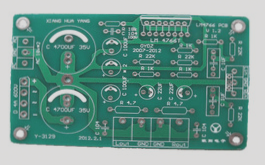
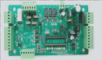
Can you clarify the specific aspects of the design you’re most concerned about—layout, wiring, or electromagnetic compatibility?

1. **Partition Method 1**
The signal line spans the gap between two grounds; what is the return path for the signal current? Assuming the two divided grounds connect at a single point somewhere, the ground current will form a large loop and flow through it. High-frequency currents generate radiation and high inductance. Low-level analog currents can be easily disturbed by external signals if they flow through such a loop. When split grounds are connected at the power supply, a large current loop forms. Moreover, connecting analog and digital grounds through a long wire can create a dipole antenna. Understanding where and how current returns to ground is key to optimizing mixed-signal board designs. Many designs only consider signal current paths, ignoring the specific return path. If ground layers must be divided and routing through the gap is necessary, create a single-point connection between the divided grounds to form a bridge, then route through this bridge. This provides a direct current return path under each signal line, minimizing loop area. Signals across the gap can also be handled with optical isolators or transformers—optical isolators use optical signals, while transformers use magnetic fields. Differential signaling is another option: the signal flows in one line and returns via another, eliminating the need for ground as a return path.
2. **Dividing Method 2**
In practical work, a unified ground is generally used, dividing the PCB into analog and digital sections. Analog signals are routed in the analog area across all board layers, while digital signals are confined to the digital circuit area. Here, digital signal return currents do not flow into the analog ground. Digital-to-analog interference occurs if digital signals are routed over analog areas or vice versa. This issue arises not from a lack of split ground but from improper digital signal routing. A unified ground with partitioned digital and analog circuits and appropriate wiring can resolve complex layout issues and prevent problems from ground separation. The layout and partition of components become crucial for design quality. With proper layout, digital ground currents remain in the digital section, avoiding interference with analog signals. Thorough checking of wiring rules is essential; improper routing can undermine the circuit board design.
3. **A/D Partition**
When connecting the analog ground (AGND) and digital ground (DGND) pins of an A/D converter, manufacturers typically recommend connecting them to the same low impedance ground with short leads. Since most A/D converter chips don’t internally connect AGND and DGND, an external connection is necessary. External impedance connected to DGND introduces parasitic capacitances, coupling digital noise into the analog circuitry. Thus, both AGND and DGND pins should connect to analog ground. If only one A/D converter is present, this is straightforward. For multiple A/D converters, connecting analog and digital grounds under each converter results in multiple connection points, reducing isolation and negating the benefit. The recommended approach is to use a unified ground, divided into analog and digital sections. This layout not only adheres to IC manufacturers’ requirements but also avoids forming loop or dipole antennas on the PCB.


