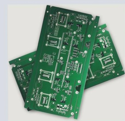
The general process of PCB board light drawing involves several steps: checking the documents, determining process parameters, transferring CAD files to Gerber format, and processing and outputting using CAM.
1. Check the documents
1.1 Check the user’s files thoroughly. The files provided by the user should undergo the following checks:
1) Ensure the integrity of the disk file.
2) Scan for viruses; eliminate any viruses detected.
3) Verify the format of user data.
4) For Gerber files, confirm the presence of a D code table or D code (RS274-X format). This necessitates a precise analysis of the data format, particularly understanding the RS274D format in Gerber. A thorough comprehension of standard Aperture is crucial, including detailed analysis of their relationships. Careful examination of the Aperture file is vital, as it may contain special cases. For instance, users might request Aperture changes from a circle to a rectangle or from a rectangle to a heat sink. The original Gerber file only contains D codes and coordinates, lacking information on size and shape. To compensate, an Aperture file is necessary. By effectively combining these files, one can accurately interpret the user’s original data.

Check whether the design conforms to the technical level of our PCB board factory
1) Check whether the various spacings designed in the customer’s documents conform to the factory’s process, including the spacing between lines, lines and pads, and pads and pads. These spacings should be greater than what the factory production process can achieve.
2) Verify the wire width, ensuring it is within the capabilities of the production process.
3) Confirm the size of via holes to match the production process capabilities.
4) Monitor the size of pads and their internal apertures to ensure adequate pad edge width after drilling.
Determine the process parameters
Various process parameters are determined based on user requirements as follows:
2.1 Determine if the photo-painted negative should be a mirror image:
– The film surface must be directly attached to the photosensitive adhesive film surface to reduce errors.
– For screen printing or dry film processes, the film surface of the negative film should align with the copper surface of the substrate. Conversely, for diazo film exposure, the film surface should not be attached to the copper surface.
– Additional mirroring is necessary for unit negatives or imposed photopainted negatives.
2.2 Establish parameters for solder mask pattern expansion:
– Ensure the solder mask pattern covers the wire next to pads but does not expose them. Adjust the pattern to avoid covering pads.
– Consider deviation values in the solder mask process and select appropriate expansion values based on different processes.
– Add process wires for gold plating needs (gold fingers) on the board.
– Include a conductive frame for electroplating and process wires for hot air leveling (tin spraying).
– Add center holes of pads and positioning holes based on drilling and subsequent process requirements.
– Include contour lines according to the board shape and adjust line widths for high precision board requirements.
Output the bottom plate light drawing
Prepare the light drawing output by adjusting the parameters of the light plotter and setting details for the light source intensity, drawing speed, negative placement, and maintenance of the table top.
The drawing of the graphic base plate involves generating light drawing data, ensuring accuracy and adherence to design requirements for different components like circuit chips, solder mask, character slices, drilling slices, and copper-clad power supply and stratum. Consider mirror drawing, graphic level identification, and aperture matching for a successful drawing process.
1. Check the documents
1.1 Check the user’s files thoroughly. The files provided by the user should undergo the following checks:
1) Ensure the integrity of the disk file.
2) Scan for viruses; eliminate any viruses detected.
3) Verify the format of user data.
4) For Gerber files, confirm the presence of a D code table or D code (RS274-X format). This necessitates a precise analysis of the data format, particularly understanding the RS274D format in Gerber. A thorough comprehension of standard Aperture is crucial, including detailed analysis of their relationships. Careful examination of the Aperture file is vital, as it may contain special cases. For instance, users might request Aperture changes from a circle to a rectangle or from a rectangle to a heat sink. The original Gerber file only contains D codes and coordinates, lacking information on size and shape. To compensate, an Aperture file is necessary. By effectively combining these files, one can accurately interpret the user’s original data.

Check whether the design conforms to the technical level of our PCB board factory
1) Check whether the various spacings designed in the customer’s documents conform to the factory’s process, including the spacing between lines, lines and pads, and pads and pads. These spacings should be greater than what the factory production process can achieve.
2) Verify the wire width, ensuring it is within the capabilities of the production process.
3) Confirm the size of via holes to match the production process capabilities.
4) Monitor the size of pads and their internal apertures to ensure adequate pad edge width after drilling.
Determine the process parameters
Various process parameters are determined based on user requirements as follows:
2.1 Determine if the photo-painted negative should be a mirror image:
– The film surface must be directly attached to the photosensitive adhesive film surface to reduce errors.
– For screen printing or dry film processes, the film surface of the negative film should align with the copper surface of the substrate. Conversely, for diazo film exposure, the film surface should not be attached to the copper surface.
– Additional mirroring is necessary for unit negatives or imposed photopainted negatives.
2.2 Establish parameters for solder mask pattern expansion:
– Ensure the solder mask pattern covers the wire next to pads but does not expose them. Adjust the pattern to avoid covering pads.
– Consider deviation values in the solder mask process and select appropriate expansion values based on different processes.
– Add process wires for gold plating needs (gold fingers) on the board.
– Include a conductive frame for electroplating and process wires for hot air leveling (tin spraying).
– Add center holes of pads and positioning holes based on drilling and subsequent process requirements.
– Include contour lines according to the board shape and adjust line widths for high precision board requirements.
Output the bottom plate light drawing
Prepare the light drawing output by adjusting the parameters of the light plotter and setting details for the light source intensity, drawing speed, negative placement, and maintenance of the table top.
The drawing of the graphic base plate involves generating light drawing data, ensuring accuracy and adherence to design requirements for different components like circuit chips, solder mask, character slices, drilling slices, and copper-clad power supply and stratum. Consider mirror drawing, graphic level identification, and aperture matching for a successful drawing process.


