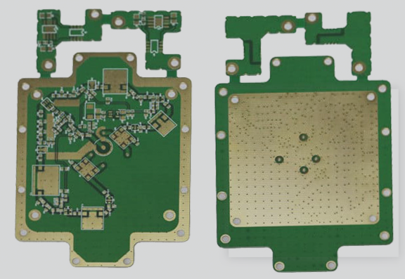
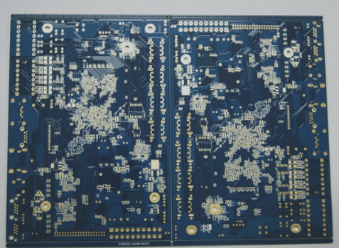
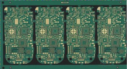
Common Causes of Poor Soldering in PCB Design
- Particulate impurities in the plating layer or grinding debris left on the circuit board surface.
- Contamination with grease, impurities, or residual silicone oil.
- Areas on the board surface lacking tin with particulate impurities in the plating layer.
- Rough high-potential coating, signs of burning, and areas without tin.
- Severely oxidized tin surface, dull copper surface in certain areas.
- Inconsistent plating between board sides, distinct bright edges around holes.
- Clear bright edges on low-potential holes, rough high-potential coating.
- Insufficient soldering temperature or time, improper flux usage.
- Inadequate tin plating coverage, dark red areas on the board surface.
Causes of Poor Tinning on Circuit Boards
- Unbalanced bath composition, low current density, insufficient plating time.
- Inadequate number and uneven distribution of anodes.
- Low or excessive concentration of tinting agent.
- Large anode size, high current density, improper wire density in certain areas.
- Residual film or organic matter before plating.
- High current density, inadequately filtered plating solution.
Strategies to Improve PCB Electro-Tinning Defects
- Regular chemical analyses and timely syrup composition adjustments.
- Periodic monitoring of anode consumption and adding anodes as needed.
- Hearst cell analysis for light agent adjustment.
- Rational anode distribution, proper current density reduction, and wiring design.
- Enhanced pre-plating treatments.
- Reduced current density, regular maintenance of the filter system.
- Strict control of storage time and environmental conditions.
- Use of solvents for debris cleaning and specialized solvents for silicone oil.
- Precise temperature control during soldering (55-80°C) with sufficient preheating.
- Proper application of soldering flux.
Understanding and addressing these issues are crucial in the PCB industry to ensure high-quality soldering and tinning processes.