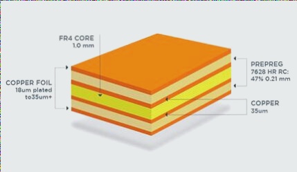
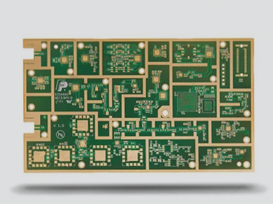
1. When drawing PCBs, it’s common sense to use thick lines for high current (such as 50mil or above) and thin lines for low current (such as 10mil). However, for electromechanical control systems, the instantaneous current flowing through the wire can sometimes exceed 100A, making thinner wires prone to problems.
2. A basic rule of thumb is 10A per square mm, meaning a wire with a cross-sectional area of 1 square mm can safely carry 10A. If the line width is too thin, it may burn out when subjected to a large current. Additionally, the current causing wire burnout should adhere to the energy formula: (Q = I^2 times t). For instance, a 30mil wire can withstand a sudden surge of 100A current lasting for a short duration.
3. Another concern is the stray inductance of the wire. This can generate a strong reverse electromotive force under the influence of an inductor, potentially damaging other devices. The longer and thinner the wire, the greater the stray inductance, necessitating consideration of wire length in practical applications.
4. General PCB design software typically offers various options for laying copper on through-hole solder pads of device pins, including right-angle spokes, 45-degree spokes, and straight spokes. Novices might overlook the significance of these choices, opting for aesthetics over functionality.
5. However, there are two primary considerations: heat dissipation and current capacity. Straight spokes provide robust current capacity but facilitate rapid heat dissipation, making soldering challenging. In contrast, right-angled and 45-degree spokes reduce the contact area between the pin and the copper foil, allowing slower heat dissipation and easier soldering.
6. Therefore, the choice of through-hole pad connection mode should be based on application requirements, considering both overcurrent capacity and heat dissipation. While low-power signal lines may not require straight spokes, high-current pads necessitate them. The choice between right-angle and 45-degree spokes is primarily aesthetic.
7. This issue came to my attention while studying a motor driver. The H bridge component repeatedly failed, baffling me for years. After extensive investigation, I discovered that the use of right-angled spokes in laying copper on a device’s solder pad in the power loop reduced the circuit’s overcurrent capacity.
8. Though the product functioned normally under typical conditions with a 10A current, a short circuit in the H bridge caused a surge of approximately 100A, immediately burning out the two spokes (in microseconds). This led to a cascading failure, damaging the control chip and power supply of the entire device.
9. Why were only two spokes used on the solder pad in the power loop? Why not allow the copper foil to go straight through? Production personnel cited difficulties in soldering the pin, prompting the designer’s decision.
10. This discovery greatly expanded my understanding, reminiscent of defusing a complex situation with a simple solution. If the VIA hole is less than 0.3mm, mechanical drilling is infeasible. Laser drilling, although possible, complicates plate production. Thus, unless absolutely necessary, a minimum diameter of 0.5mm outside/0.3mm inside is recommended.
11. However, certain components like computer motherboards, memory chips, and dense BGA packages may require smaller holes, sometimes as small as 14mil/8mil. The hole diameter generally equals 1.5 times the line width, although special applications like power supply may deviate from this rule.


