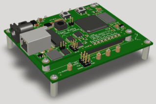
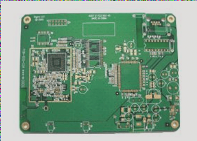
In high-speed PCB, circuit wiring is more than just connecting two points. As a qualified engineer, wiring is a hybrid knowledge vehicle that includes resistors, capacitors, and inductors. It is necessary to understand that the reflection of the signal line during transmission depends on the Z of the transmission line and the Z of the load.
The magnitude of the reflected signal is measured by the reflection coefficient KR. The reflection coefficient at the load end is KRL=(ZL-Z0)/(ZL+Z0). For open-circuit load, KRL=1; For short circuit loads, KRL=-1 is visible, for open and short circuit loads, the signal is 100% reflected back. A negative KRL indicates that the reflected signal is in the opposite direction from the original signal. Similarly, the magnitude of the reflection of the signal at the source end is expressed as the reflection coefficient at the source end: KRS=(ZS-Z0)/(ZS+Z0).
Sets the standard output level of the drive to 0.2 V, current 24 ma, ZS about 8.3Ω its output impedance. Set the input impedance of load ZL is larger than 100 k Ω than Z0 (about 67 Ω), the load end reflection coefficient is: the KRL = 1, the signal was 100% at the load end reflection. The reflection coefficient at the source end is KRS=-0.78.
Below is a detailed analysis of the driver to generate a switch from 3.5V to 0.2V signal reflection process.
The first reflection: the driver voltage is 3.3V, according to the ZS and Z0 component of the voltage principle, the signal △V=-2.94V generated on Z0, the signal voltage at the source end is VS=O.56V. The reflection coefficient at the load end is 1. When the signal reaches the load end, VL=3.5-2.94-2.94=-2.38V.
The second reflection: the signal at the source end is 0.56V at the beginning, when the -2.94V signal reaches the source end, the second reflection occurs, and the reflected voltage is: VR=KPS*△V =-0.78*(-2.94)=2.29V. So the voltage at the source end becomes VS=0.56+ (-2.94) +2.29=-0.09V.
Third reflection: When the second reflection signal reaches the load end, the load end voltage becomes VL =-2.38+2.29+2.29=2.2.V.
On such a mismatched impedance transmission line, the signal is reflected back and forth in this way, with each reflection decreasing in amplitude until it finally disappears. The vertical lines on the left and right represent the voltages at the source and the load, respectively, and the diagonal lines indicate the voltages of the transmitted and reflected signals. It can also be used to represent the specific reflection process of the signal, one represents the source side signal, one represents the load side signal. It can be seen that only after 5 cycles do the signal transmitted to the load end drop below the input threshold value, and the transmission delay is generally between 6 — 16ns/m. If the transmission delay tPD=10ns/m, then the transmission delay through a 0.15m transmission line is about 1.5ns, then the signal can be considered effective after about 13.5ns is transmitted.


