PCB Manual Wiring and Design Tips
Wiring is a critical aspect of PCB design, involving the connection of components using traces and vias. Altium Designer offers advanced tools like interactive routing and the Situs topology auto-router to streamline the routing process.
While automatic routing is efficient, manual routing provides greater control over trace placement, ideal for complex designs or those preferring a hands-on approach. This tutorial focuses on manual routing, specifically routing traces on the bottom layer of a PCB.
PCB Routing Tutorial Using Altium Designer
Routing traces is a key step in PCB design, with straight segments and defined angles for a professional layout. Here’s a guide to routing on the bottom layer:
- Displaying the Bottom Layer: Use shortcut key **L** to open **View Configurations** and enable the Bottom Layer for visibility.
- Starting Interactive Routing: Go to **Place >> Interactive Routing** or use shortcut **P, T** to activate the routing tool.
- Initiating the Routing Process: Begin at the starting point and proceed to route the trace following the desired path.
- Routing the Trace: Choose between Auto-Complete (CTRL + Click) for automatic completion or Manual Routing for precise control.
- Line Status: Dashed lines indicate unplaced traces, while solid lines show placed traces, aiding in tracking progress.
- Routing Additional Connections
By following these steps, you can effectively route traces on the bottom layer of your PCB design in Altium Designer.
Routing Between Components on the Board
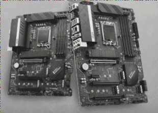
To continue routing between other components on the board, use the methods mentioned above. As you route several traces, your design will start resembling the manually wired board shown in the tutorial’s figure.
Saving Your Design
After completing your routing, remember to save your progress by pressing **F, S** or **Ctrl + S**.
Handling Obstacles with Interactive Routing Modes
Altium Designer’s interactive routing tool offers various modes to resolve conflicts and obstacles during routing. You can switch between these modes by pressing **Shift + R**. The available modes include:
- **Push Mode**: Moves objects to make room for new traces.
- **Walkaround Mode**: Finds a path to bypass obstacles without moving them.
- **Hug & Push Mode**: Combines features of Walkaround and Push modes.
- **Ignore Mode**: Allows free routing without considering obstacles.
If routing faces obstacles that prevent completion, Altium Designer will prompt you immediately, indicating the issue.
Useful Shortcuts and Tips for Efficient Routing
- **Enter/Click**: Place a trace at the cursor position.
- **CTRL + Click**: Use Auto-Complete for fast routing between pads on the same layer.
- **Shift + R**: Cycle through routing modes.
- **Shift + Spacebar**: Switch between line angle modes.
- **END Key**: Refresh the screen.
- **V, F**: Re-adjust the screen to fit all objects in view.
- **Page Up/Page Down**: Zoom in or out.
- **Backspace**: Cancel the previous trace placement.
- **ESC**: Exit the routing mode.
Preventing Mistakes in Connectivity
Altium Designer constantly monitors board connectivity to prevent unintended connections between pins that should not be joined, reducing common errors during the design process.
Deleting or Rewiring Traces
To delete or rewire traces, select the trace and press **Delete**. If a trace is incorrectly placed, right-click and choose **Delete** to remove it. Altium Designer will automatically clear redundant segments upon finishing routing.
Exiting Routing Mode
Once all connections are made, right-click or press **ESC** to exit the routing mode. By following these steps and utilizing Altium Designer’s routing tools, you can efficiently route your PCB traces, manage obstacles, and ensure clean, error-free designs.