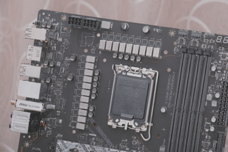
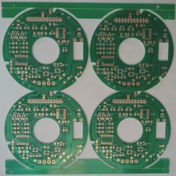
1. The definition of high-frequency PCBs in circuit board production. A high-frequency board is a specialized circuit board designed to operate at elevated electromagnetic frequencies, utilized in high-frequency (greater than 300 MHz or wavelengths shorter than 1 meter) and microwave (greater than 3 GHz or wavelengths shorter than 0.1 meter) applications.
2. High-frequency PCBs are produced on microwave-grade copper-clad substrates, employing some processes typical of standard rigid circuit board manufacturing or specialized techniques.
3. In general terms, a high-frequency board can be categorized as one that operates above 1 GHz.
4. With the rapid advancement of science and technology, an increasing number of devices are engineered for use in the microwave frequency range (above 1 GHz) or even in the millimeter-wave spectrum (up to 30 GHz).
5. This progression indicates that operating frequencies are on the rise, necessitating higher material standards for circuit boards.
6. For instance, substrate materials must possess outstanding electrical characteristics, good chemical stability, and minimal loss as signal frequencies increase, thereby underscoring the significance of high-frequency boards.
7. Applications of high-frequency PCBs include mobile communication devices, power amplifiers, low-noise amplifiers, and passive components such as power splitters, couplers, duplexers, and filters.
8. Additionally, they are integral to automotive collision avoidance systems, satellite communication, radio systems, and other domains, reflecting the trend toward increased frequencies in electronic equipment.
1. The application fields for PCB high-frequency boards include mobile communication products, power amplifiers, low-noise amplifiers, and passive components like power splitters, couplers, duplexers, and filters.
2. They are also utilized in automotive anti-collision systems, satellite systems, radio systems, and other electronic fields, making high-frequency equipment a significant development trend.
3. High-frequency board classifications include ceramic-filled thermosetting materials such as Rogers’ 4350B/4003C, Arlon’s 25N/25FR, and Taconic’s TLG series.
4. The processing method for circuit boards resembles that of epoxy resin/glass woven cloth (FR4), though the sheets are relatively brittle and prone to breakage.
5. Drilling and machining can reduce the lifespan of drill tips and cutting tools by approximately 20%.
6. PTFE (polytetrafluoroethylene) materials are sourced from manufacturers like Rogers (RO3000 series, RT series, TMM series), Arlon (AD/AR series), and others.
7. The processing method involves careful cutting, ensuring the protective film remains to avoid scratches.
8. For drilling, utilize a brand-new drill bit (standard 130), applying a pressure of 40 psi on the presser foot, with aluminum sheets as cover plates.
9. After drilling, use an air gun to clear dust from the holes, employing stable drilling rigs and parameters for optimal results.
10. Hole processing can benefit from plasma treatment or sodium naphthalene activation for better metallization.
11. For PTH sinking copper, begin after micro-etching, controlling the micro-etch rate to 20 microinches, and then pull the board from the de-oiler cylinder.
12. If necessary, a second PTH can be performed, starting from the anticipated cylinder.
13. The solder mask process starts with acidic plate washing instead of mechanical grinding, followed by baking the plate at 90°C for 30 minutes.
14. This is followed by three stages of baking at 80°C, 100°C, and 150°C, each for 30 minutes; rework may be needed if the substrate is oily.
15. For the gong board process, place white paper on the PTFE surface, clamping it with FR-4 substrates or phenolic plates.
16. Burrs on the back of the gong board must be trimmed carefully to protect the substrate and copper surface.
17. To minimize burrs, effective gong board processing is crucial.
18. The NPTH PTFE sheet processing flow includes cutting, drilling, dry film application, inspection, etching, erosion inspection, solder mask application, character printing, tin spraying, forming, testing, final inspection, packaging, and shipment.
19. The PTH PTFE plate processing flow follows a similar sequence but includes hole treatment and copper immersion before the dry film application.
**Summarize the difficulties of high-frequency circuit board processing**
1. **Immersion copper:** Achieving copper coverage on the hole wall is challenging.
2. **Control of line gaps:** Managing the gaps and sand holes during image transfer, etching, and line width is critical.
3. **Green oil process:** Ensuring adhesion of the green oil and controlling its foaming is essential.
4. **Surface integrity:** Maintaining a strict control over board surface scratches throughout each processing stage is necessary.
—
Let me know if you need anything else!