
PCB Ceramic Substrate Manufacturing Technology
Introduction
PCB production facilities utilize various ceramic manufacturing technologies, with over 30 distinct processes involved. Common methods include dry pressing, slurry casting, extrusion, injection molding, seeding, and isostatic pressing.
Dry Pressing Method
One of the primary techniques used in PCB ceramic substrate manufacturing is dry pressing. This method is preferred for its simplicity and cost-effectiveness. The process involves three key stages: green body formation, sintering, and circuit creation.
Green Body Formation
In the green body formation stage, high-purity alumina powder (typically 95% Al2O3) is used. The powder is mixed with additives like binders and dispersants to create a slurry for shaping.
- Dry compaction uses high-purity alumina powder with an alumina content over 92%.
- For dry compaction, particle size should not exceed 60 µm.
- The dry-pressed blank can be processed before sintering, such as adjusting shape and size.
Casting Method
Another method for creating the green body is through the casting method. A liquid mixture of aluminum oxide powder, solvents, dispersants, adhesives, and plasticizers is used. The process involves mixing, sieving, expansion flow, drying, trimming, and sintering.
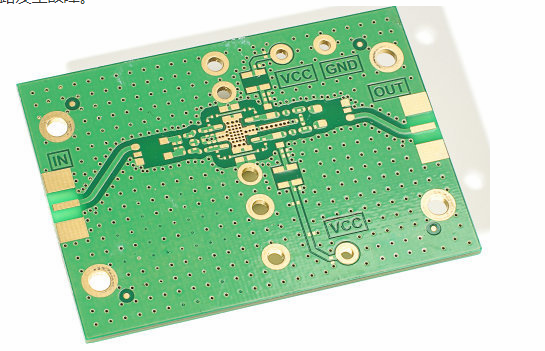
PCB Design Schematic Drawing Skills
When designing PCB schematics, it’s essential to pay attention to common errors that may arise during the process.
Common Errors in PCB Schematics
- ERC reports no access signal for this pin: This error can occur due to incorrectly defined I/O attributes for pins during package creation.
- ERC reports duplicate network tags: This error may be caused by connecting different network labels together or assigning multiple labels to the same connection.
- The component runs outside the graphic boundary: Components should not be placed outside the center of the component library sheet.
- The created project file netlist only partially adjusts to the PCB: Ensure the netlist is generated with the global option selected.
- Avoid using comments when creating custom multi-part components.
By understanding these common errors and solutions, PCB designers can enhance the quality and accuracy of their schematic drawings.

 العربية
 简体中文
简体中文 Nederlands
 English
 Français
 Deutsch
 Italiano
 日本語
日本語 한국어
한국어 Português
 Русский
 Español
 ไทย
ไทย