Eight-Layer Circuit Board Manufacturing Process
Introduction to Eight-Layer Circuit Boards
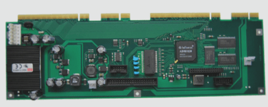
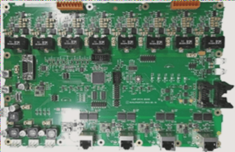
Eight-layer circuit boards are essential components in the PCB industry, offering high wiring density and the ability to accommodate components on both sides. They have replaced single-sided PCBs and paved the way for multi-layer PCB technology, providing high-performance solutions for electronic products.
Wiring Method for Eight-Layer Circuit Boards
An eight-layer PCB typically includes top and bottom layers for signal lines, along with internal layers for power planes like VCC and GND. The wiring process involves adding internal planes and middle layers to connect power and ground planes, crucial for routing multi-layer signal lines.
Preventing Copper Foil Creasing
- Thicker copper foils help prevent creasing in PCB multilayer boards.
- Proper substrate layout and control of adhesive flow during melting are key factors.
- Using elastic carrier plates with adjustable mechanisms can prevent copper foil shifting.
- Choosing films with lower adhesive content and controlling pressing parameters can reduce creasing risks.
Processing Flow for Eight-Layer Circuit Boards
- Eight-layer copper-clad board blanking
- Drilling of reference and via holes
- Inspection and deburring
- Plating processes for metallization
- Application of circuit patterns and solder resist graphics
- Final inspection, packaging, and shipment
Following these steps ensures the production of high-precision eight-layer circuit boards for various electronic applications.
Advanced PCB Technology: Understanding Eight-Layer PCBs
When it comes to advanced PCB technology, eight-layer PCBs are a popular choice. These PCBs are designed to accommodate complex circuitry by providing multiple layers for routing signals. One key feature of eight-layer PCBs is the inclusion of vias and blind vias.
What are Vias and Blind Vias?
Vias are holes that run from the top layer to the bottom layer of the PCB. They are used to establish connections between different layers of the board. On the other hand, blind vias are visible only from one of the outer layers (top or bottom). These vias do not penetrate through all layers of the PCB; instead, they are drilled from the surface but stop before reaching the inner layers.
The Role of Buried Vias
In addition to blind vias, there are also buried vias. These vias are located within the inner layers of the PCB, making them invisible from both the top and bottom layers. By utilizing buried and blind vias, PCB designers can maximize the available routing space on the board, allowing for more efficient and compact designs.
Advantages of Using Buried and Blind Vias
- Increased routing space
- Complex circuitry support
- Improved signal integrity
Overall, the use of buried and blind vias in eight-layer PCBs offers numerous benefits, making them a popular choice for high-density and high-performance applications.