Introduction:
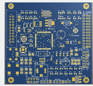
The demand for high-density flexible substrates in miniaturized and high-performance packaging devices has led to the increasing use of the semi-additive process over the subtractive process.
Semi-Additive Process:
The traditional subtractive method used in flexible substrate circuit formation faces limitations due to side etching. To address this issue, the semi-additive process has gained popularity in creating high-precision circuits.
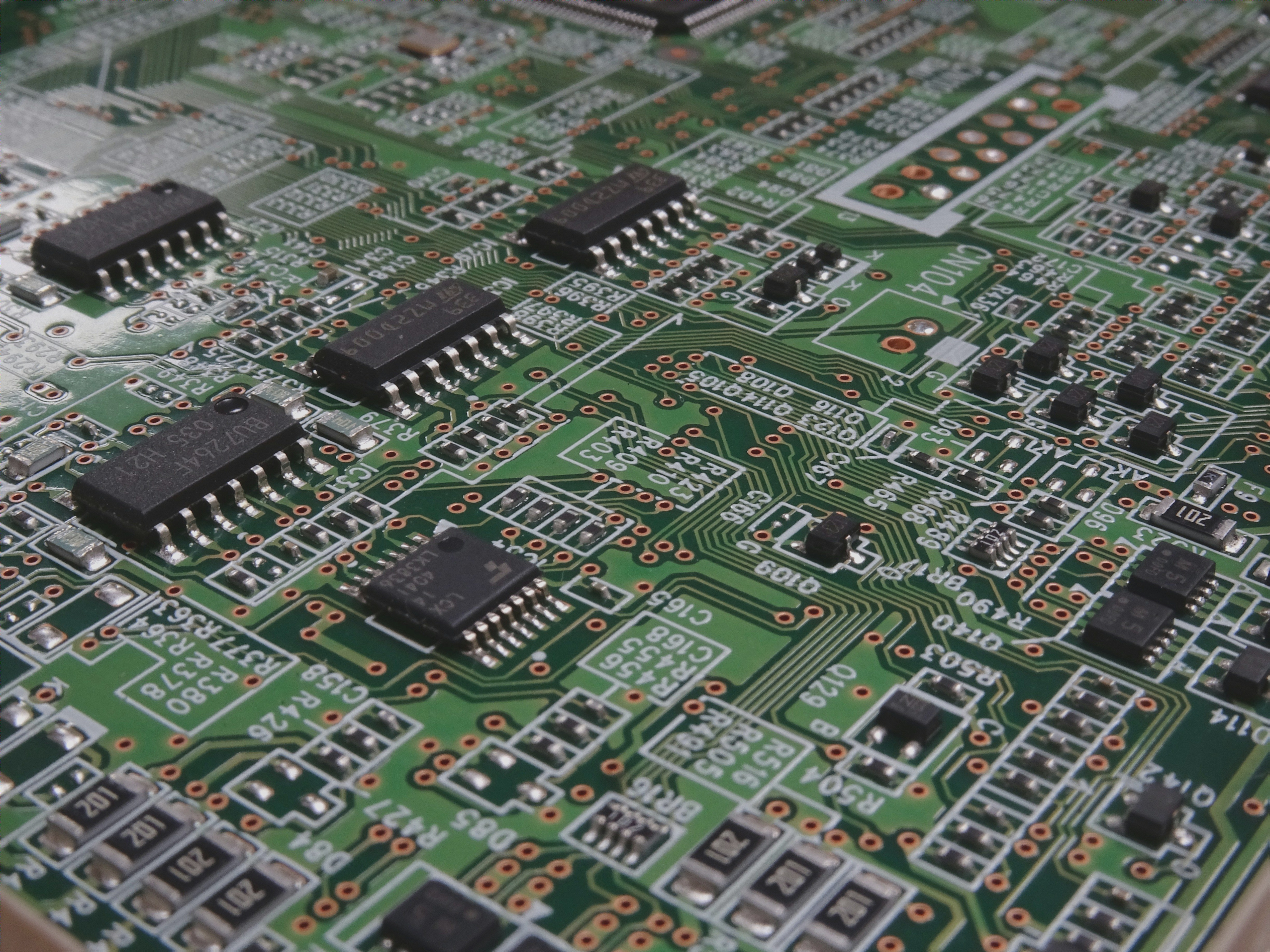
Copper foil is commonly employed in the industry to reduce side etching effects. However, decreasing copper thickness can lead to increased DC resistance, affecting high-speed signal transmission negatively.
In contrast, the semi-additive process forms conductive patterns by plating within photoresist openings, offering high-density and high-speed capabilities simultaneously.
The main steps of the semi-additive process include:
- Applying a metal buffer layer through sputtering onto the polyimide substrate.
- Using image transfer technology to create a plating-resistant dry film pattern on the buffer layer.
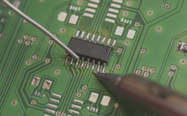
- Electroplating to thicken copper conductor lines.
- Utilizing differential etching to fabricate the line layer.
Achieving consistent thickness and strong adhesion of the buffer layer to the substrate and dry film is crucial, requiring continuous testing and process optimization.
Ultrathin Flexible Substrate Manufacturing Process:
As electronic devices continue to shrink in size, reducing chip sizes to 50μm or thinner has become a trend. Flexible substrates offer advantages over rigid ones by reducing stress-induced chip damage through their ability to bend with the chip.
For any inquiries regarding PCBs and PCBA, please reach out to info@wellcircuits.com.