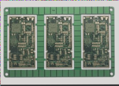
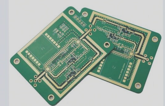
Partially buried daughter board technology can reduce material costs for manufacturing multi-structure interconnected PCBs. However, challenges persist such as difficulties in bypassing the daughter board during processing, poor alignment, issues with glue overflow on the board surface, and significant board warping. This article addresses these issues and proposes solutions including design improvements for aligning the daughter board’s rounded corners, precise copper cutting to control overflow, and optimizing the laminated structure to mitigate board warping. These measures aim to enhance product quality and manufacturing yield.
As the price of PCB raw materials continues to rise, effective cost control in product manufacturing grows increasingly crucial. In cases requiring the integration and compression of special materials, a proven approach involves segregating the special material wiring section into an independent layer. However, this method can hinder product thickness reduction and underutilize the special material area. A more innovative approach involves local embedding of daughter boards using special materials as independent substrates, integrating them with conventional materials to form a composite laminate structure.

Therefore, the thickness of the product can be further reduced. Additionally, special materials are utilized as independent sub-boards to maximize their efficiency, thereby reducing material costs and optimizing space.
However, in actual product applications, the adoption of local buried sub-board technology remains limited, with the original independent hierarchical structure using special materials still prevailing. Despite the potential cost savings offered by local sub-board technology, challenges persist in controlling the production process. Consequently, many manufacturers prefer to adopt more conventional approaches to mitigate technical risks.
To address the challenges associated with local buried sub-board processing and reduce technical risks, this article aims to thoroughly analyze the underlying issues and propose practical and effective processing solutions for reference.
The typical manufacturing process of partially buried daughter board PCB resembles that of most embedded products. Throughout this process, particular attention is given to pre- and post-press stages of the motherboard, emphasizing precise alignment of the PCB daughter board. Key control requirements typically include:
(1) Ensuring that the layer offset between the PCB daughter board and the motherboard after pressing does not exceed 0.075mm;
(2) Completely filling any gaps between the PCB daughter board and the motherboard with adhesive, ensuring no voids, and limiting the width of adhesive flow onto the copper surface to no more than 0.1mm;
(3) Post-press, the height difference of the filled edge surface should not exceed 0.1mm, and the board warping should be controlled within 0.75%.
As the price of PCB raw materials continues to rise, effective cost control in product manufacturing grows increasingly crucial. In cases requiring the integration and compression of special materials, a proven approach involves segregating the special material wiring section into an independent layer. However, this method can hinder product thickness reduction and underutilize the special material area. A more innovative approach involves local embedding of daughter boards using special materials as independent substrates, integrating them with conventional materials to form a composite laminate structure.

Therefore, the thickness of the product can be further reduced. Additionally, special materials are utilized as independent sub-boards to maximize their efficiency, thereby reducing material costs and optimizing space.
However, in actual product applications, the adoption of local buried sub-board technology remains limited, with the original independent hierarchical structure using special materials still prevailing. Despite the potential cost savings offered by local sub-board technology, challenges persist in controlling the production process. Consequently, many manufacturers prefer to adopt more conventional approaches to mitigate technical risks.
To address the challenges associated with local buried sub-board processing and reduce technical risks, this article aims to thoroughly analyze the underlying issues and propose practical and effective processing solutions for reference.
The typical manufacturing process of partially buried daughter board PCB resembles that of most embedded products. Throughout this process, particular attention is given to pre- and post-press stages of the motherboard, emphasizing precise alignment of the PCB daughter board. Key control requirements typically include:
(1) Ensuring that the layer offset between the PCB daughter board and the motherboard after pressing does not exceed 0.075mm;
(2) Completely filling any gaps between the PCB daughter board and the motherboard with adhesive, ensuring no voids, and limiting the width of adhesive flow onto the copper surface to no more than 0.1mm;
(3) Post-press, the height difference of the filled edge surface should not exceed 0.1mm, and the board warping should be controlled within 0.75%.


