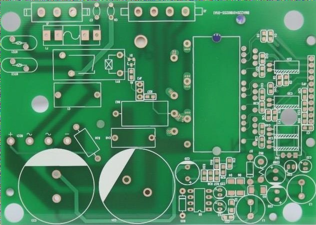
1. The resin plug hole is a widely used and favored process in recent years, especially for high-precision multilayer PCB boards and products with large thickness.
2. However, some problems that cannot be solved by using green oil plug hole and pressing resin filling are hoped to be resolved by the resin plug hole.
3. Due to the characteristics of the resin itself, many difficulties need to be overcome in the production of the circuit board to improve the quality of the resin plug hole.

1. The production of outer layer shall meet the requirements of negative film, and the thickness diameter ratio of through-hole shall be ≤ 6:1.
Negative film requirements shall meet the following conditions:
1) The line width/line gap is large enough
2) The maximum PTH hole is less than the maximum sealing capacity of dry film
3) The PCB thickness is less than the maximum thickness required by the negative film.
4) Plates without special requirements, such as: local electroplated gold plate, nickel plated gold plate, half hole plate, printed plug board, non ring PTH hole, plates with PTH slot hole, etc. Fabrication of inner layer of PCB board — pressing — browning — laser drilling — browning reduction — outer layer drilling — copper sinking — whole board hole filling electroplating — slice analysis — outer layer graphics — outer layer acid etching — outer layer AOI — subsequent normal process.
2. The production of outer layer shall meet the requirements of negative film, and the thickness diameter ratio of through-hole shall be more than 6:1.
As the thickness diameter ratio of through-hole is greater than 6:1, the requirements for through-hole copper thickness can not be met by using the whole plate for hole filling electroplating. After the whole plate for hole filling electroplating, it is necessary to use an ordinary electroplating line to plate the through-hole copper to the required thickness, The specific operation process is as follows: production of inner layer — pressing — browning — laser drilling — browning reduction — outer layer drilling — copper sinking — whole plate hole filling electroplating — whole plate electroplating — slice analysis — outer layer graphics — outer layer acid etching — subsequent normal process.
3. The outer layer does not meet the negative film requirements, the line width/line gap is ≥ a, and the thickness diameter ratio of the outer layer through-hole is less than or equal to 6:1. Fabrication of the inner layer of the printed circuit boards — pressing — browning — laser drilling — browning reduction — outer layer drilling — copper sinking — hole filling electroplating of the whole board — slice analysis — outer layer graphics — pattern electroplating — outer layer alkaline etching — outer layer AOI — subsequent normal process.
4. The outer layer does not meet the negative film requirements, and the line width/line gap is less than a; Or line width/line gap ≥ a, thickness diameter ratio of through-hole more than 6:1. Production of inner layer — pressing — browning — laser drilling — browning reduction — copper sinking — hole filling electroplating of the whole plate — slicing analysis — copper reduction — outer layer drilling — copper sinking — full plate electroplating — outer layer graphics — graphics electroplating — outer layer alkaline etching — outer layer AOI — subsequent normal process. The manufacturing process of the resin plug hole of PCB board: first drill holes, then plate the holes, then bake the resin plug hole, and finally grind (grind). The resin after being polished does not contain copper, so it needs to be turned into PAD on a layer of copper. This step was done before the original PCB drilling process. First, the holes to be plugged were treated, and then other holes were drilled, following the original normal process. When the plug hole is not plugged properly and there are bubbles in the hole, the bubbles are likely to burst when PCB passes through the tin furnace because they are easy to absorb moisture. In the process of making the resin plug hole of PCB board, if there are bubbles in the hole, these bubbles will be discharged by the resin during baking, which will cause the situation that one side is concave and the other side is convex. We can directly detect such defective products. Of course, if the newly delivered PCB board has been baked during loading, generally, there will be no board explosion.
5. What does PCB board slotting mean?
The slotting can be drawn on the mechanical layer. The width of the slotting is the line width, and the shape of the slotting is linear. If you need a ring, use the mechanical layer to draw multiple arcs. When drawing, just indicate that the mechanical layer is a grooved layer. Between the strong and weak current on the PCB, the PCB material can also withstand a certain voltage, but after a long time of use, the PCB will be stained with dust and moisture, resulting in a reduction in the voltage withstand, which means that the creepage distance is reduced. Note: Creepage distance refers to the phenomenon that the insulation resistance decreases after the insulator surface is contaminated and damped, and current (even arc) is generated under high voltage. Between the high voltages of components, PCB slotting can only be used to prevent insufficient creepage distance and increased leakage current of PCB when it is wet. After the PCB board is grooved, direct air isolation is used for short distance, and the withstand voltage of the electrical gap will be guaranteed to a certain extent. Slotting under the transformer is to allow better heat dissipation of the transformer and reduce EMC radiation caused by distributed capacitance. The dielectric strength is the best in solid or liquid, such as diode PN junction, MOS tube insulating grid, transformer oil. For example, the bushing of the power transformer is not big in diameter and the distance between the core column and the transformer shell is not big, but because it is in the transformer oil and ceramics, it can withstand very high voltage (the bushing is quite long, and the surface is made of ripples and grooves to increase the distance along the surface). Then comes the normal temperature and pressure or high-pressure gas. The worst dielectric strength is the solid, because the solid surface will be contaminated with dust and moisture.
We hope that some knowledge about the PCB board resin plug hole making process and PCB slotting can help you!
2. However, some problems that cannot be solved by using green oil plug hole and pressing resin filling are hoped to be resolved by the resin plug hole.
3. Due to the characteristics of the resin itself, many difficulties need to be overcome in the production of the circuit board to improve the quality of the resin plug hole.

1. The production of outer layer shall meet the requirements of negative film, and the thickness diameter ratio of through-hole shall be ≤ 6:1.
Negative film requirements shall meet the following conditions:
1) The line width/line gap is large enough
2) The maximum PTH hole is less than the maximum sealing capacity of dry film
3) The PCB thickness is less than the maximum thickness required by the negative film.
4) Plates without special requirements, such as: local electroplated gold plate, nickel plated gold plate, half hole plate, printed plug board, non ring PTH hole, plates with PTH slot hole, etc. Fabrication of inner layer of PCB board — pressing — browning — laser drilling — browning reduction — outer layer drilling — copper sinking — whole board hole filling electroplating — slice analysis — outer layer graphics — outer layer acid etching — outer layer AOI — subsequent normal process.
2. The production of outer layer shall meet the requirements of negative film, and the thickness diameter ratio of through-hole shall be more than 6:1.
As the thickness diameter ratio of through-hole is greater than 6:1, the requirements for through-hole copper thickness can not be met by using the whole plate for hole filling electroplating. After the whole plate for hole filling electroplating, it is necessary to use an ordinary electroplating line to plate the through-hole copper to the required thickness, The specific operation process is as follows: production of inner layer — pressing — browning — laser drilling — browning reduction — outer layer drilling — copper sinking — whole plate hole filling electroplating — whole plate electroplating — slice analysis — outer layer graphics — outer layer acid etching — subsequent normal process.
3. The outer layer does not meet the negative film requirements, the line width/line gap is ≥ a, and the thickness diameter ratio of the outer layer through-hole is less than or equal to 6:1. Fabrication of the inner layer of the printed circuit boards — pressing — browning — laser drilling — browning reduction — outer layer drilling — copper sinking — hole filling electroplating of the whole board — slice analysis — outer layer graphics — pattern electroplating — outer layer alkaline etching — outer layer AOI — subsequent normal process.
4. The outer layer does not meet the negative film requirements, and the line width/line gap is less than a; Or line width/line gap ≥ a, thickness diameter ratio of through-hole more than 6:1. Production of inner layer — pressing — browning — laser drilling — browning reduction — copper sinking — hole filling electroplating of the whole plate — slicing analysis — copper reduction — outer layer drilling — copper sinking — full plate electroplating — outer layer graphics — graphics electroplating — outer layer alkaline etching — outer layer AOI — subsequent normal process. The manufacturing process of the resin plug hole of PCB board: first drill holes, then plate the holes, then bake the resin plug hole, and finally grind (grind). The resin after being polished does not contain copper, so it needs to be turned into PAD on a layer of copper. This step was done before the original PCB drilling process. First, the holes to be plugged were treated, and then other holes were drilled, following the original normal process. When the plug hole is not plugged properly and there are bubbles in the hole, the bubbles are likely to burst when PCB passes through the tin furnace because they are easy to absorb moisture. In the process of making the resin plug hole of PCB board, if there are bubbles in the hole, these bubbles will be discharged by the resin during baking, which will cause the situation that one side is concave and the other side is convex. We can directly detect such defective products. Of course, if the newly delivered PCB board has been baked during loading, generally, there will be no board explosion.
5. What does PCB board slotting mean?
The slotting can be drawn on the mechanical layer. The width of the slotting is the line width, and the shape of the slotting is linear. If you need a ring, use the mechanical layer to draw multiple arcs. When drawing, just indicate that the mechanical layer is a grooved layer. Between the strong and weak current on the PCB, the PCB material can also withstand a certain voltage, but after a long time of use, the PCB will be stained with dust and moisture, resulting in a reduction in the voltage withstand, which means that the creepage distance is reduced. Note: Creepage distance refers to the phenomenon that the insulation resistance decreases after the insulator surface is contaminated and damped, and current (even arc) is generated under high voltage. Between the high voltages of components, PCB slotting can only be used to prevent insufficient creepage distance and increased leakage current of PCB when it is wet. After the PCB board is grooved, direct air isolation is used for short distance, and the withstand voltage of the electrical gap will be guaranteed to a certain extent. Slotting under the transformer is to allow better heat dissipation of the transformer and reduce EMC radiation caused by distributed capacitance. The dielectric strength is the best in solid or liquid, such as diode PN junction, MOS tube insulating grid, transformer oil. For example, the bushing of the power transformer is not big in diameter and the distance between the core column and the transformer shell is not big, but because it is in the transformer oil and ceramics, it can withstand very high voltage (the bushing is quite long, and the surface is made of ripples and grooves to increase the distance along the surface). Then comes the normal temperature and pressure or high-pressure gas. The worst dielectric strength is the solid, because the solid surface will be contaminated with dust and moisture.
We hope that some knowledge about the PCB board resin plug hole making process and PCB slotting can help you!


