Multi-Layer PCB Board Design: Key Considerations
- Multi-layer PCBs: Understanding the Basics
- Advantages of Multi-Layer PCB Boards
- Design Principles for Multi-Layer PCB Boards
- Optimizing Component Placement on Multi-Layer Boards
- Efficient Wire Layout Strategies for Multi-Layer PCBs
- Ensuring Signal Integrity in Multi-Layer PCB Designs
- Importance of Safety Distances in Multi-Layer PCBs
- Enhancing Anti-Interference Capability in Multi-Layer PCBs
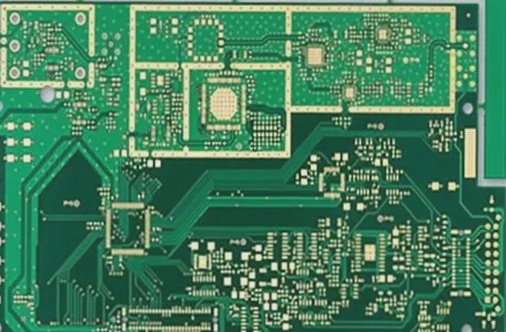
Multi-layer PCB boards are a crucial component in modern electronics, offering numerous advantages over single-sided or double-sided boards. These boards, consisting of multiple layers of connecting wires and insulating substrates, provide high assembly density, faster signal transmission, and effective shielding.
When designing multi-layer PCB boards, symmetry, proper component placement, wire layout, safety distances, and anti-interference measures are essential considerations. Ensuring a balanced distribution of power, ground, and signal layers, as well as optimizing the orientation of traces, can significantly impact the board’s performance and reliability.
Engineers should also pay attention to safety standards, incorporating filter capacitors, shielded wires, and appropriate grounding points to enhance anti-interference capabilities. By following these design principles and best practices, multi-layer PCB boards can meet the demands of complex electronic systems while maintaining efficiency and reliability.
For more information on multi-layer PCB fabrication and design, visit Wellcircuits.