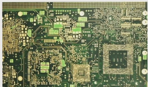
With the continuous miniaturization, increasing precision, and higher speeds of electronic products, PCB design has evolved to meet more complex requirements. It no longer simply involves establishing the circuit connections between components; it must also address the various challenges posed by high-speed and high-density designs. Today, high-speed PCB design is an essential skill that every practitioner in the PCB design industry must master to remain competitive.
### Transmission Line Concept
A transmission line is a signal pathway that includes both a signal path and a signal return path. Typically, this consists of two conductive traces: one for signal propagation and the other for signal return. In PCB design, the most common form of transmission line is the trace on the PCB itself. These traces must be carefully designed to ensure signal integrity, especially as signal speeds increase and the layout becomes denser. Proper management of transmission lines is critical in minimizing signal degradation and interference, especially for high-speed circuits.
### Design Challenges in High-Speed PCBs
As the demand for faster, smaller, and more complex circuits grows, PCB designers face several challenges, including managing signal reflections, minimizing crosstalk, and preventing signal loss. In high-speed designs, the transmission lines must be treated as an integral part of the circuit, requiring precise control of trace length, impedance, and routing. Signal integrity analysis and impedance matching are key factors in successful high-speed PCB design.
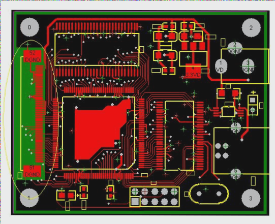
High-density designs further complicate the task by increasing the number of traces and components within the same physical area, requiring careful routing and layer management. Designers must strike a balance between functionality, manufacturability, and performance, using advanced simulation tools to predict and mitigate potential issues before fabrication.
### Conclusion
High-speed PCB design has become a critical skill in the modern electronics industry, where the performance of a product depends heavily on the precise management of signal integrity. As technology continues to advance, mastering the concepts of transmission lines and understanding their role in high-density, high-speed designs will remain essential for success in PCB design.

The two most common types of transmission lines in digital PCB design are microstrip and stripline, each serving distinct purposes depending on the design and performance requirements.
### Microstrip Lines
Microstrip lines are typically found on the outer layers of the PCB and are characterized by having only one reference plane, usually the ground. There are two types of microstrip lines:
1. **Non-buried Microstrip**: These are simply the traces on the outer layer with the ground layer serving as the reference plane.
2. **Buried (or Submerged) Microstrip**: In this configuration, the transmission line is embedded within the PCB’s dielectric layers, but it still only has a single reference plane.
### Stripline
On the other hand, a stripline refers to the transmission lines that are routed on the inner layers of the PCB, sandwiched between two reference planes—typically, a ground plane and a power plane. This design offers better isolation from external electromagnetic interference (EMI) and enhances signal integrity compared to microstrip lines, especially in high-speed designs.
**Transmission Line Selection for High-Speed Designs**
In high-speed PCB designs, especially those with four or more layers, it’s generally preferable to use stripline routing for critical signals. This helps reduce electromagnetic interference (EMI) and improves electromagnetic compatibility (EMC), while also boosting the design’s resistance to external noise.
### Signal Delay and Its Impact
Signal delay, also referred to as transmission delay, is a crucial factor in high-speed designs. It occurs because signals travel at a finite speed along the PCB traces, causing a time lag between the signal’s transmission and reception. The delay is influenced by two main factors:
– **Trace Length**: The longer the transmission line, the greater the delay.
– **Dielectric Constant**: The type of material surrounding the traces also affects the signal speed, with different materials introducing varying levels of delay.
In high-speed digital systems, the length of the signal transmission line directly impacts the phase difference of the clock pulses. This phase difference occurs when two clock signals, generated simultaneously, arrive at the receiving end at different times, disrupting synchronization. If the phase difference is too large, timing errors can occur, leading to system malfunctions.
In such cases, the delay introduced by transmission lines can become a critical part of the overall clock cycle, influencing the timing of the signal edges and, consequently, the performance of the system.
### Serial vs. Parallel Buses
High-speed signals are commonly found in both serial and parallel buses, each with distinct wiring considerations. Understanding the nature of the bus—whether serial or parallel—and its operating speed is essential before routing the PCB traces.
1. **Serial Bus**: In serial communication, data is transmitted one bit at a time, allowing for longer transmission distances with fewer lines. Although the bits are transmitted sequentially, the differential pair configuration (positive and negative traces) is typically used in high-speed serial communication to improve noise immunity and signal integrity. Length matching is generally not a concern, as each bit is independent, though signal timing must still be considered.
2. **Parallel Bus**: In parallel communication, multiple bits are transmitted simultaneously, meaning that each signal line in the group must maintain synchronization. A common example of a parallel bus is DDR memory, which uses multiple data lines (e.g., D0-D7) along with control signals like DQS and DQM. For proper data transmission, all these lines must be of equal length to avoid misalignment and ensure that all bits arrive at the receiving end at the same time. Even a slight delay in one bit could cause incorrect data transmission, necessitating retransmission.
**Key Design Consideration**: For parallel buses, careful attention must be given to trace length matching to ensure the simultaneous arrival of signals, whereas for serial buses, the length of the differential pairs is less critical, though still important for maintaining signal integrity.
### Conclusion
In summary, both microstrip and stripline transmission lines play important roles in high-speed PCB designs. Stripline is preferred for high-speed signals in multi-layer PCBs due to its superior shielding from external interference, while microstrip lines are typically used for less critical, outer-layer routing. Understanding the impact of signal delay and the characteristics of the bus (serial or parallel) is vital for optimizing the PCB design, ensuring signal integrity, and preventing timing errors. Proper trace routing, especially for parallel buses, is crucial to maintain synchronization and data reliability.
### Transmission Line Concept
A transmission line is a signal pathway that includes both a signal path and a signal return path. Typically, this consists of two conductive traces: one for signal propagation and the other for signal return. In PCB design, the most common form of transmission line is the trace on the PCB itself. These traces must be carefully designed to ensure signal integrity, especially as signal speeds increase and the layout becomes denser. Proper management of transmission lines is critical in minimizing signal degradation and interference, especially for high-speed circuits.
### Design Challenges in High-Speed PCBs
As the demand for faster, smaller, and more complex circuits grows, PCB designers face several challenges, including managing signal reflections, minimizing crosstalk, and preventing signal loss. In high-speed designs, the transmission lines must be treated as an integral part of the circuit, requiring precise control of trace length, impedance, and routing. Signal integrity analysis and impedance matching are key factors in successful high-speed PCB design.
High-density designs further complicate the task by increasing the number of traces and components within the same physical area, requiring careful routing and layer management. Designers must strike a balance between functionality, manufacturability, and performance, using advanced simulation tools to predict and mitigate potential issues before fabrication.
### Conclusion
High-speed PCB design has become a critical skill in the modern electronics industry, where the performance of a product depends heavily on the precise management of signal integrity. As technology continues to advance, mastering the concepts of transmission lines and understanding their role in high-density, high-speed designs will remain essential for success in PCB design.
The two most common types of transmission lines in digital PCB design are microstrip and stripline, each serving distinct purposes depending on the design and performance requirements.
### Microstrip Lines
Microstrip lines are typically found on the outer layers of the PCB and are characterized by having only one reference plane, usually the ground. There are two types of microstrip lines:
1. **Non-buried Microstrip**: These are simply the traces on the outer layer with the ground layer serving as the reference plane.
2. **Buried (or Submerged) Microstrip**: In this configuration, the transmission line is embedded within the PCB’s dielectric layers, but it still only has a single reference plane.
### Stripline
On the other hand, a stripline refers to the transmission lines that are routed on the inner layers of the PCB, sandwiched between two reference planes—typically, a ground plane and a power plane. This design offers better isolation from external electromagnetic interference (EMI) and enhances signal integrity compared to microstrip lines, especially in high-speed designs.
**Transmission Line Selection for High-Speed Designs**
In high-speed PCB designs, especially those with four or more layers, it’s generally preferable to use stripline routing for critical signals. This helps reduce electromagnetic interference (EMI) and improves electromagnetic compatibility (EMC), while also boosting the design’s resistance to external noise.
### Signal Delay and Its Impact
Signal delay, also referred to as transmission delay, is a crucial factor in high-speed designs. It occurs because signals travel at a finite speed along the PCB traces, causing a time lag between the signal’s transmission and reception. The delay is influenced by two main factors:
– **Trace Length**: The longer the transmission line, the greater the delay.
– **Dielectric Constant**: The type of material surrounding the traces also affects the signal speed, with different materials introducing varying levels of delay.
In high-speed digital systems, the length of the signal transmission line directly impacts the phase difference of the clock pulses. This phase difference occurs when two clock signals, generated simultaneously, arrive at the receiving end at different times, disrupting synchronization. If the phase difference is too large, timing errors can occur, leading to system malfunctions.
In such cases, the delay introduced by transmission lines can become a critical part of the overall clock cycle, influencing the timing of the signal edges and, consequently, the performance of the system.
### Serial vs. Parallel Buses
High-speed signals are commonly found in both serial and parallel buses, each with distinct wiring considerations. Understanding the nature of the bus—whether serial or parallel—and its operating speed is essential before routing the PCB traces.
1. **Serial Bus**: In serial communication, data is transmitted one bit at a time, allowing for longer transmission distances with fewer lines. Although the bits are transmitted sequentially, the differential pair configuration (positive and negative traces) is typically used in high-speed serial communication to improve noise immunity and signal integrity. Length matching is generally not a concern, as each bit is independent, though signal timing must still be considered.
2. **Parallel Bus**: In parallel communication, multiple bits are transmitted simultaneously, meaning that each signal line in the group must maintain synchronization. A common example of a parallel bus is DDR memory, which uses multiple data lines (e.g., D0-D7) along with control signals like DQS and DQM. For proper data transmission, all these lines must be of equal length to avoid misalignment and ensure that all bits arrive at the receiving end at the same time. Even a slight delay in one bit could cause incorrect data transmission, necessitating retransmission.
**Key Design Consideration**: For parallel buses, careful attention must be given to trace length matching to ensure the simultaneous arrival of signals, whereas for serial buses, the length of the differential pairs is less critical, though still important for maintaining signal integrity.
### Conclusion
In summary, both microstrip and stripline transmission lines play important roles in high-speed PCB designs. Stripline is preferred for high-speed signals in multi-layer PCBs due to its superior shielding from external interference, while microstrip lines are typically used for less critical, outer-layer routing. Understanding the impact of signal delay and the characteristics of the bus (serial or parallel) is vital for optimizing the PCB design, ensuring signal integrity, and preventing timing errors. Proper trace routing, especially for parallel buses, is crucial to maintain synchronization and data reliability.