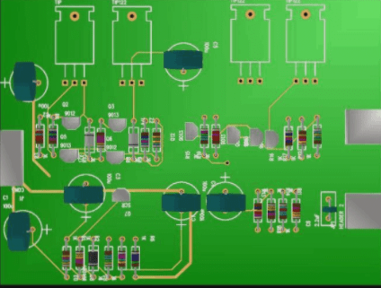
PCB board copying, also known as circuit board copying, cloning, reverse engineering, or reverse R&D, involves analyzing existing electronic products and circuit boards using reverse R&D technology. The goal is to translate the PCB board and bill of materials (BOM) documents from the original product into 1:1 technical documents, including parts, schematic documents, PCB screen printing production documents, and other technical documents. These technical and production documents are then used for PCB manufacturing, component welding, flying probe testing, and PCB debugging in order to complete the replication of the original PCB template.

Many people are unfamiliar with the concept of PCB copying. Some even mistake it for plagiarism. However, PCB copying is not about imitation, but rather about learning from foreign electronic circuit design technology, absorbing the design scheme, and using it to develop more products. As the PCB industry continues to evolve, the concept of PCB copying has expanded to include not only simple circuit board copying and cloning, but also the secondary development and research of new products. By analyzing existing product technical documents, design ideas, structural characteristics, and process technology, we can provide feasibility analyses and competitive references for the development and design of new products. This can assist in following technology trends, adjusting and improving product design, and developing new products with market competitiveness. The PCB copying process can also facilitate the rapid updating, upgrading, and secondary development of various types of electronic products through the extraction and partial modification of technical documents.
The PCB schematic diagram plays a pivotal role in both reverse research and forward design. Reverse engineering the schematic diagram of a PCB requires several steps, attention to detail, and thorough testing. To begin, record all PCB related details and take scanned images of the top and bottom layers. These images must be adjusted and corrected in Photoshop to ensure a clear depiction of the PCB.
It’s essential to verify the position coincidence of pads and vias in the layers to ensure the accuracy of the previous steps. The next steps involve painting the layers, combining the top and bottom layers, and laser printing the layers on transparent film to compare with the original PCB. Finally, thorough testing is necessary to verify the electronic technical performance of the board.
When reverse designing the schematic diagram, it’s important to reasonably divide functional areas and use reference pieces for accurate schematic drawing. Additionally, correctly distinguishing lines and plotting wiring is crucial to ensure clear identification and avoid crossing or interpenetration. It’s also essential to master the basic framework and learn from similar schematic diagrams, as well as to thoroughly check and optimize the schematic diagram once completed. Attention to these details can ensure the accuracy and success of the PCB copying process.


