What are the characteristics of PCBA?
I believe many people are familiar with PCB circuit boards, as they are commonly mentioned in daily life. However, they might not know much about PCBA and may even confuse it with PCB. So, what exactly is a PCB? How did PCBA come about? What distinguishes PCB from PCBA? Let’s explore these topics in detail below.
About PCB
PCB stands for Printed Circuit Board, which translates into Chinese as “印刷电路板.” It is called a “printed” circuit board because it is produced through electronic printing methods. PCBs are essential electronic components in the electronics industry, serving as supports for electronic components and as carriers for electrical connections. Their applications in manufacturing electronic products are vast. The unique characteristics of PCBs can be summarized as follows:
1. High wiring density, compact size, and lightweight design, which facilitate the miniaturization of electronic devices.
2. The repeatability and consistency of the graphics reduce wiring and assembly errors, thereby saving time during maintenance, debugging, and inspection.
3. They promote mechanization and automation in production, enhancing labor productivity and lowering costs for electronic devices.
4. PCB design can be standardized, which enhances interchangeability.

**About PCBA**
PCBA stands for Printed Circuit Board Assembly, which signifies that PCBA undergoes the complete manufacturing process from PCB blank board through SMT (Surface Mount Technology) and then DIP (Dual In-line Package) assembly.
**Note:** SMT and DIP are both techniques for integrating components onto the PCB. The primary distinction is that SMT does not require drilling holes in the PCB, whereas DIP necessitates that the component pins be inserted into pre-drilled holes.
SMT primarily utilizes automated mounters to place small components onto the PCB. The production process involves: positioning the PCB, printing solder paste, mounting components with the mounter, passing through a reflow oven, and conducting final inspection. In contrast, DIP, which stands for “plug-in,” involves inserting components into the PCB. This method is used for larger components that are not suitable for surface mounting. The main steps in this process include applying adhesive, inserting components, inspection, wave soldering, and final inspection.
*The Difference Between PCB and PCBA*
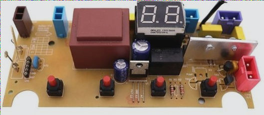
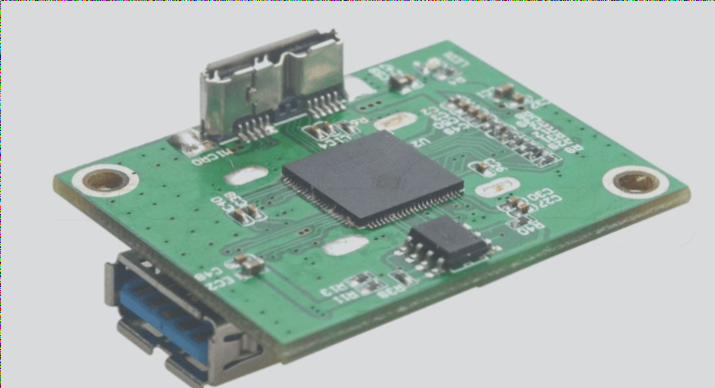
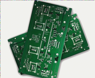
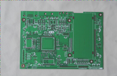
From the aforementioned discussion, we can conclude that PCBA typically refers to a processing stage and can also be viewed as a completed circuit board. In contrast, PCB denotes a bare printed circuit board without any components.
In summary: PCBA is a finished board; PCB is a bare board.
**Materials Used in the Circuit Board Manufacturing Process in PCBA**
1. **Substrate**
The fundamental material for printed circuit boards is a copper-clad substrate, commonly referred to as the substrate. This is a resin board with copper layers on both sides. The most widely used type is FR-4, which is primarily utilized in computers, communication equipment, and various other electronic products. Key requirements for the board include flame resistance, the glass transition temperature (Tg), and the dielectric constant. The circuit board must be flame-resistant, meaning it will not ignite at certain temperatures but will only soften.
2. **Copper Foil**
Copper foil acts as the conductor that forms the wiring on the substrate. There are two methods for producing copper foil: rolling and electrolysis.
3. **PP**
PP is a vital raw material in circuit board production, serving as the adhesive between layers. In simpler terms, the substrate sheet in the B-stage is referred to as PP. The specifications for PP include thickness and the amount of adhesive (resin).
4. **Dry Film**
Photosensitive dry film, or simply dry film, is primarily composed of resin materials that react to specific wavelengths of light through photochemical processes. A typical dry film consists of three layers, with the photosensitive layer sandwiched between two protective plastic films. There are two categories of dry films: photopolymerizable and photodegradable. The photopolymerizable dry film hardens when exposed to specific light wavelengths, transforming from a water-soluble to a water-insoluble substance, while the photodegradable film behaves oppositely.
5. **Solder Resist Paint**
Solder resist is a type of protective coating that prevents solder from adhering to undesired areas. It is a liquid photosensitive material that exhibits no affinity for liquid solder. Similar to photosensitive dry film, solder resist hardens under specific light wavelengths. It is mixed with a hardener before application and is often referred to as ink. The colors we typically see on circuit boards are actually the colors of the solder resist.
6. **Film**
The negatives mentioned here are analogous to photographic negatives; they utilize photosensitive materials to record images. Customers provide their designed circuit diagrams to the PCB factory, where the CAM (Computer-Aided Manufacturing) workstation outputs the circuit diagrams using a light plotter instead of a standard printer. The film plays a crucial role in the circuit board manufacturing process, as all image transfer techniques require the creation of a film prior to application on the substrate.
If you have any PCB manufacturing needs, please do not hesitate to contact me.Contact me
I believe many people are familiar with PCB circuit boards, as they are commonly mentioned in daily life. However, they might not know much about PCBA and may even confuse it with PCB. So, what exactly is a PCB? How did PCBA come about? What distinguishes PCB from PCBA? Let’s explore these topics in detail below.
About PCB
PCB stands for Printed Circuit Board, which translates into Chinese as “印刷电路板.” It is called a “printed” circuit board because it is produced through electronic printing methods. PCBs are essential electronic components in the electronics industry, serving as supports for electronic components and as carriers for electrical connections. Their applications in manufacturing electronic products are vast. The unique characteristics of PCBs can be summarized as follows:
1. High wiring density, compact size, and lightweight design, which facilitate the miniaturization of electronic devices.
2. The repeatability and consistency of the graphics reduce wiring and assembly errors, thereby saving time during maintenance, debugging, and inspection.
3. They promote mechanization and automation in production, enhancing labor productivity and lowering costs for electronic devices.
4. PCB design can be standardized, which enhances interchangeability.
**About PCBA**
PCBA stands for Printed Circuit Board Assembly, which signifies that PCBA undergoes the complete manufacturing process from PCB blank board through SMT (Surface Mount Technology) and then DIP (Dual In-line Package) assembly.
**Note:** SMT and DIP are both techniques for integrating components onto the PCB. The primary distinction is that SMT does not require drilling holes in the PCB, whereas DIP necessitates that the component pins be inserted into pre-drilled holes.
SMT primarily utilizes automated mounters to place small components onto the PCB. The production process involves: positioning the PCB, printing solder paste, mounting components with the mounter, passing through a reflow oven, and conducting final inspection. In contrast, DIP, which stands for “plug-in,” involves inserting components into the PCB. This method is used for larger components that are not suitable for surface mounting. The main steps in this process include applying adhesive, inserting components, inspection, wave soldering, and final inspection.
*The Difference Between PCB and PCBA*
From the aforementioned discussion, we can conclude that PCBA typically refers to a processing stage and can also be viewed as a completed circuit board. In contrast, PCB denotes a bare printed circuit board without any components.
In summary: PCBA is a finished board; PCB is a bare board.
**Materials Used in the Circuit Board Manufacturing Process in PCBA**
1. **Substrate**
The fundamental material for printed circuit boards is a copper-clad substrate, commonly referred to as the substrate. This is a resin board with copper layers on both sides. The most widely used type is FR-4, which is primarily utilized in computers, communication equipment, and various other electronic products. Key requirements for the board include flame resistance, the glass transition temperature (Tg), and the dielectric constant. The circuit board must be flame-resistant, meaning it will not ignite at certain temperatures but will only soften.
2. **Copper Foil**
Copper foil acts as the conductor that forms the wiring on the substrate. There are two methods for producing copper foil: rolling and electrolysis.
3. **PP**
PP is a vital raw material in circuit board production, serving as the adhesive between layers. In simpler terms, the substrate sheet in the B-stage is referred to as PP. The specifications for PP include thickness and the amount of adhesive (resin).
4. **Dry Film**
Photosensitive dry film, or simply dry film, is primarily composed of resin materials that react to specific wavelengths of light through photochemical processes. A typical dry film consists of three layers, with the photosensitive layer sandwiched between two protective plastic films. There are two categories of dry films: photopolymerizable and photodegradable. The photopolymerizable dry film hardens when exposed to specific light wavelengths, transforming from a water-soluble to a water-insoluble substance, while the photodegradable film behaves oppositely.
5. **Solder Resist Paint**
Solder resist is a type of protective coating that prevents solder from adhering to undesired areas. It is a liquid photosensitive material that exhibits no affinity for liquid solder. Similar to photosensitive dry film, solder resist hardens under specific light wavelengths. It is mixed with a hardener before application and is often referred to as ink. The colors we typically see on circuit boards are actually the colors of the solder resist.
6. **Film**
The negatives mentioned here are analogous to photographic negatives; they utilize photosensitive materials to record images. Customers provide their designed circuit diagrams to the PCB factory, where the CAM (Computer-Aided Manufacturing) workstation outputs the circuit diagrams using a light plotter instead of a standard printer. The film plays a crucial role in the circuit board manufacturing process, as all image transfer techniques require the creation of a film prior to application on the substrate.
If you have any PCB manufacturing needs, please do not hesitate to contact me.Contact me

