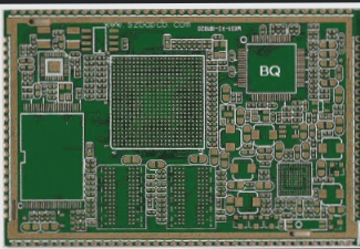
Understanding Multi-Layer PCBs: Enhancing Electronic Functionality
- PCBs come in various forms: single-sided, double-sided, and multi-layered.
- Single-sided PCBs are suitable for basic devices like radios.
- As technology advances, complex electronics require multi-layer PCBs.
- Multi-layer PCBs offer advantages like high assembly density and effective shielding.
- There is virtually no limit to the number of layers in multi-layer boards.
Optimizing Multi-Layer PCB Design
In multi-layer PCB design, symmetry is crucial to prevent distortions. Wiring should adhere to functional requirements, prioritizing connections on the soldering surface for maintenance ease.
Segregating power, ground, and signal layers minimizes interference. Perpendicular or oblique lines between adjacent layers reduce coupling and interference.
Distinct Layers in Multi-Layer PCBs
- Signal Layers: Route electrical signals for component communication.
- Internal Planes: Distribute power efficiently and maintain stable voltage.
- Mechanical Layers: Provide structural support for rigidity and durability.
- Masks: Shield the PCB from environmental factors and aid in soldering.
- Silkscreen: Add labels and visual indicators for component placement.
- System Layer: Integrate components and functionalities for system operation.
Enhanced Functionality with Multi-Layer PCBs
By incorporating distinct layers, multi-layer PCBs offer improved functionality, performance, and reliability compared to single or double-sided boards. Each layer contributes to the overall efficiency and effectiveness of the PCB, making it a versatile solution for various electronic applications.
Signal and Power Layers in Multi-Layer PCBs
The signal layer is divided into top, middle, and bottom layers for component placement, wiring, and soldering. The internal power layer routes power lines and ground connections efficiently.
The Mechanical Layer in PCB Design
The mechanical layer in PCB design provides crucial information regarding board fabrication and assembly methods. This includes details on circuit board dimensions, data references, and through-hole specifications.
Top and Bottom Layers for PCB Layout
PCBs have top and bottom layers designated for pad placement and areas without copper traces. These layers play a key role in ensuring proper functionality and connectivity of the circuit board.
Significance of Screen Printing Layer
The screen printing layer in PCB design is essential for outlining components, displaying component identifiers, and providing textual information. It aids in the visual representation and organization of components on the board.
Importance of System Working Layer
The system working layer in PCB design is crucial as it highlights any violations of design rules. This layer helps designers identify and rectify any issues that may impact the performance or functionality of the printed circuit board.