PCB Copper Foil Substrate Quality Control
The demand for PCB copper foil substrates is increasing as electronic systems require lighter, thinner, and more reliable products. Manufacturers must adhere to strict quality standards, considering factors such as raw materials, glue content, and pressing conditions. To maintain quality control, facilities are adopting non-contact laser measurement systems, replacing manual inspections.
Transition to Laser Measurement Systems
PCB copper foil substrate manufacturers are shifting towards non-contact laser thickness measurement systems to enhance quality control. These systems offer unique features and require integration with on-site design and construction. By implementing laser technology, manufacturers can improve accuracy and efficiency in measuring thickness.
Importance of Thickness Quality
The thickness of PCB copper foil substrates directly impacts the reliability of electronic products. In the past, meeting IPC-4101 CLASS B standards sufficed, but the industry now demands CLASS C or higher for advanced circuit boards. Statistical Process Control (SPC) metrics like process accuracy (Ca) and process capability index (Cpk) are utilized to ensure products meet specifications.
Enhancing Process Capability
SPC focuses on improving in-plant processes to maintain product quality within specification limits. Negotiating Cpk values and specifications between suppliers and manufacturers is crucial to avoid costly errors. By understanding Cpk data and conducting screening tests, manufacturers can enhance process stability and product quality.
- Quality Control Factors: raw materials, glue content, pressing conditions
- Transition to Laser Measurement Systems for accuracy and efficiency
- Importance of Thickness Quality in electronic product reliability
- Utilization of Statistical Process Control (SPC) for process improvement
Board Edge Measurement and Classification
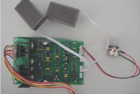
Traditionally, board edges were measured manually using micrometers, posing challenges for complete inspection. To address this issue, a laser thickness gauge with a non-contact laser displacement sensor was developed. Compliance with IPC regulations is essential, with Class A products labeled with red and Class B with blue labels. For customers with stricter requirements, sub-station processing can categorize products into four levels and stacks.
Architecture of Thickness Gauge
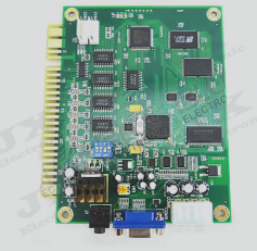
The thickness gauge, designed with a laser displacement sensor, combines optical and mechanical components. The optical design functions as a standalone sensor part, enabling simple electromechanical integration, while software expansion is crucial. Figure 3 demonstrates the architectural flow of the thickness gauge, emphasizing the critical selection and interconnection of components to prevent errors and instability.
Displacement Sensor Selection
- Consider PCB copper foil substrate characteristics for displacement sensor selection.
- Compare measurement distance, resolution, linearity, and sampling period.
- Ensure measurement distance covers all PCB substrates; align resolution with sensor specs.
- Higher resolution with fewer samples indicates better performance.
- Lower linearity is preferred for accuracy.
Analog-to-Digital Conversion Card Criteria
- Focus on 16-bit resolution for thin-plate market applications.
- Consider input channel requirements and voltage range.
- Most designs need six input channels for three profiles.
- ADC cards handle up to 16 channels with voltage and current output signals.
Digital Card Functions
- Digital I/O cards operate with binary values of 0 and 1.
- DI signals include counters and photoelectric switches for substrate detection.
- DO signals facilitate control, quality analysis results display, and alarms.
- Analog-to-digital conversion and digital card functions can be combined into a multifunction I/O card.
Theory and Maintenance
Ongoing maintenance and improvements are necessary due to aging equipment or evolving customer requirements. Analyzing theoretical aspects helps identify abnormalities and ensure equipment reliability.
Conclusion
The PCB copper foil substrate laser thickness measurement system integrates various components like the laser displacement sensor, mechanical design, circuitry, photoelectric switches, wiring, and software. Understanding the architectural process is crucial for timely fault resolution and quality control. Utilize the equipment with caution and thorough comprehension to maintain trust and system efficiency.