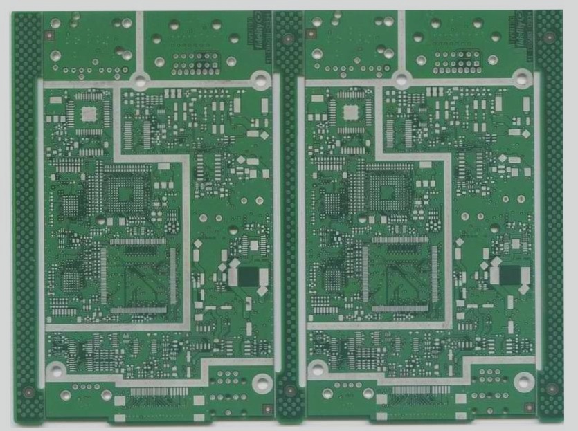
Incomplete Solder Joint in BGA Repair in FR-4 PCB
When dealing with incomplete solder joints in BGA repair on FR-4 PCBs, it typically indicates a lack of solder volume, resulting in an unreliable connection. This issue is identifiable during AXI inspection by the visibly smaller size of the solder joint compared to others.
Root Causes of Incomplete Solder Joints:
- Insufficient solder paste
- Solder cored phenomenon
- Chip or tin offset
- Missing solder mask separation
- Damage to solder mask during repair
- Incorrect design
One common consequence of insufficient solder joints is the poor coplanarity of devices and PCBs. If the solder paste quantity is adequate but the gap between BGA and FR-4 PCB is inconsistent, it can lead to incomplete solder joints.
Solutions for Insufficient Solder Joints in BGA Welding:
- Ensure sufficient solder paste application
- Cover vias with resistance welding
- Avoid damaging the solder mask
- Accurately align and print solder paste
- Ensure BGA mounting accuracy
- Operate BGA components correctly during repair
- Meet coplanarity requirements of PCB and BGA
- Utilize microporous technology to reduce solder loss
Common Problems and Welding Defects of Wave Soldering
Pulling Tip:
Causes: Improper transmission speed, low preheating temperature, inadequate tin pot temperature, poor wave crest, solder failure, and more.
Solutions: Adjust transmission speed, preheating temperature, tin pot temperature, conveyor belt angle, optimize nozzle, adjust flux, and address lead solderability.
Bridging:
Causes: Low preheating temperature, high solder copper content, flux failure, improper PCB layout, and more.
Solutions: Adjust temperatures, test solder content, optimize flux density, modify PCB design, and check PCB quality.
Faulty Soldering:
Causes: Poor lead solderability, low preheating temperature, flux issues, and more.
Solutions: Address lead solderability, adjust temperatures, test solder content, clean board surface, and more.
Thin Tin:
Causes: Poor solderability, large pad holes, fast conveyor speed, and more.
Solutions: Address solderability, adjust design, clean board surface, and ensure adequate tin content.
PCB Solutions for Common Issues
-
Solve Solderability Problems
Issues with lead wire solderability can be addressed by reducing the solder pad size, minimizing the welding angle, adjusting transmission speed, regulating tin pot temperature, checking pre-coating flux device, and testing solder Sn content.
-
Address Missing Welding
Partial welding or openings can result from various factors such as poor lead wire solderability, unstable solder wave, ineffective flux, uneven flux spraying, local PCB solderability issues, transmission chain jitter, and process flow inconsistencies. Solutions involve improving lead solderability, inspecting wave crest device, flux replacement, checking pre-coating flux device, resolving PCB solderability problems, adjusting transmission device, ensuring uniform flux application, and optimizing process flow.
-
Resolve Large Deformation of Printed Boards
Deformation in printed boards can stem from fixture failures, operational issues, uneven PCB pre-heating, high preheating and tin pot temperatures, slow transmission speed, PCB material selection, moisture in PCB storage, and PCB width discrepancies.
-
Improve Wettability
Enhancing wettability involves addressing poor solderability of components/pads, flux activity deficiencies, and inadequate preheating/tin pot temperatures. Solutions include testing component/pad solderability, changing flux, and increasing preheating/tin pot temperatures for FR-4 PCBs.