1. PCB board cutting is a critical aspect of PCB design.
2. However, many designers hesitate to engage in this task due to the challenges posed by sandpaper grinding (a hazardous process) and line drawing (a monotonous, repetitive task).
3. Many designers even perceive PCB cutting as lacking technical complexity, believing that junior designers can perform this task with minimal training.
4. While this view has some validity, it overlooks specific aspects of PCB cutting that, when mastered, can significantly save time and reduce labor efforts.
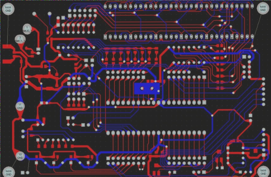
5. The concept of PCB board cutting involves obtaining the schematic and board diagrams (PCB layouts) from the original PCB.
6. The goal is to facilitate subsequent development activities, including component installation, in-depth testing, and circuit modifications.
7. Since these activities are related but distinct from PCB cutting, they will only be briefly mentioned here.
8. The PCB board cutting process begins with the removal of components from the original board.

2. Scan the original board to create a graphic file.
3. Grind off the surface layer to access the intermediate layer.
4. Scan the middle layer to produce a graphic file.
5. Repeat steps 2-4 until all layers have been processed.
6. Use specialized software to convert graphic files into electrical relationship files—PCB diagrams. With the right software, designers only need to trace the graphics once.
7. Verify and complete the design.
The cutting of PCB boards, particularly multi-layer ones, is a time-consuming and labor-intensive task that involves a significant amount of repetitive work. Designers must possess ample patience and attention to detail, as mistakes can easily occur. The key to effective PCB design lies in utilizing appropriate software to automate repetitive tasks, thereby saving time and ensuring accuracy.
1. A scanner must be employed during the cutting process.
Many designers prefer to draw lines directly in PCB design systems like PROTEL, PADS, or CAD. This practice is counterproductive. The scanned graphic file serves not only as the foundation for converting into a PCB file but also as a reference for later inspection. Utilizing scanners can significantly reduce the difficulty and intensity of labor. It is fair to say that if one fully leverages the scanner, even individuals without design experience can successfully complete PCB board cutting tasks.
2. Grind the plate in a single direction.
In the interest of speed, some designers opt for two-way grinding (removing layers from both the front and back surfaces to reach the middle layer). This approach is fundamentally flawed. Two-way grinding can easily wear through layers, leading to damage in other sections, with predictable consequences. The outer layer of the PCB is hardened due to processing, while the middle layer remains softer, which can lead to more severe issues that often cannot be polished. Additionally, the materials, hardness, and elasticity of PCBs produced by different manufacturers can vary significantly, making precise grinding challenging.
How to Choose a Suitable PCB Rapid Prototyping Manufacturer
For users seeking PCB prototyping, selecting a manufacturer that can meet their design requirements can be daunting due to an overwhelming amount of information. Here are several key points to consider when choosing a suitable PCB prototyping factory.
1. Exceptional production technology.
Opt for PCB prototyping manufacturers that offer a range of processes, such as immersion gold and lead spray tin, to ensure the quality of the circuit boards.
2. Rigorous quality supervision system.
Unlike many other products, PCB circuit boards necessitate high production accuracy. A manufacturer with a stringent supervision and management system—including IQC raw material inspections, OQC shipment testing, QE inspection standards, and QA quality assurance—indicates high product quality and is worth considering.
3. High yield rates.
Manufacturers with high yields demonstrate advanced production equipment and the capacity to produce high-quality PCB prototypes.
4. Comprehensive after-sales service.
After-sales service is a crucial factor in evaluating manufacturer quality. Choose PCB prototyping manufacturers with robust after-sales systems and strong guarantees.
5. Reputation within the industry.
A significant amount of negative feedback in the industry may suggest low user satisfaction and poor brand reputation.
6. Successful collaborations with major brands.
If a manufacturer has worked with well-known brands, it indicates rich industry experience and reliability.
By understanding these six selection criteria, you can effectively identify a suitable PCB rapid prototyping manufacturer.
If you have any PCB manufacturing needs, please do not hesitate to contact me.Contact me
2. However, many designers hesitate to engage in this task due to the challenges posed by sandpaper grinding (a hazardous process) and line drawing (a monotonous, repetitive task).
3. Many designers even perceive PCB cutting as lacking technical complexity, believing that junior designers can perform this task with minimal training.
4. While this view has some validity, it overlooks specific aspects of PCB cutting that, when mastered, can significantly save time and reduce labor efforts.
5. The concept of PCB board cutting involves obtaining the schematic and board diagrams (PCB layouts) from the original PCB.
6. The goal is to facilitate subsequent development activities, including component installation, in-depth testing, and circuit modifications.
7. Since these activities are related but distinct from PCB cutting, they will only be briefly mentioned here.
8. The PCB board cutting process begins with the removal of components from the original board.

2. Scan the original board to create a graphic file.
3. Grind off the surface layer to access the intermediate layer.
4. Scan the middle layer to produce a graphic file.
5. Repeat steps 2-4 until all layers have been processed.
6. Use specialized software to convert graphic files into electrical relationship files—PCB diagrams. With the right software, designers only need to trace the graphics once.
7. Verify and complete the design.
The cutting of PCB boards, particularly multi-layer ones, is a time-consuming and labor-intensive task that involves a significant amount of repetitive work. Designers must possess ample patience and attention to detail, as mistakes can easily occur. The key to effective PCB design lies in utilizing appropriate software to automate repetitive tasks, thereby saving time and ensuring accuracy.
1. A scanner must be employed during the cutting process.
Many designers prefer to draw lines directly in PCB design systems like PROTEL, PADS, or CAD. This practice is counterproductive. The scanned graphic file serves not only as the foundation for converting into a PCB file but also as a reference for later inspection. Utilizing scanners can significantly reduce the difficulty and intensity of labor. It is fair to say that if one fully leverages the scanner, even individuals without design experience can successfully complete PCB board cutting tasks.
2. Grind the plate in a single direction.
In the interest of speed, some designers opt for two-way grinding (removing layers from both the front and back surfaces to reach the middle layer). This approach is fundamentally flawed. Two-way grinding can easily wear through layers, leading to damage in other sections, with predictable consequences. The outer layer of the PCB is hardened due to processing, while the middle layer remains softer, which can lead to more severe issues that often cannot be polished. Additionally, the materials, hardness, and elasticity of PCBs produced by different manufacturers can vary significantly, making precise grinding challenging.
How to Choose a Suitable PCB Rapid Prototyping Manufacturer
For users seeking PCB prototyping, selecting a manufacturer that can meet their design requirements can be daunting due to an overwhelming amount of information. Here are several key points to consider when choosing a suitable PCB prototyping factory.
1. Exceptional production technology.
Opt for PCB prototyping manufacturers that offer a range of processes, such as immersion gold and lead spray tin, to ensure the quality of the circuit boards.
2. Rigorous quality supervision system.
Unlike many other products, PCB circuit boards necessitate high production accuracy. A manufacturer with a stringent supervision and management system—including IQC raw material inspections, OQC shipment testing, QE inspection standards, and QA quality assurance—indicates high product quality and is worth considering.
3. High yield rates.
Manufacturers with high yields demonstrate advanced production equipment and the capacity to produce high-quality PCB prototypes.
4. Comprehensive after-sales service.
After-sales service is a crucial factor in evaluating manufacturer quality. Choose PCB prototyping manufacturers with robust after-sales systems and strong guarantees.
5. Reputation within the industry.
A significant amount of negative feedback in the industry may suggest low user satisfaction and poor brand reputation.
6. Successful collaborations with major brands.
If a manufacturer has worked with well-known brands, it indicates rich industry experience and reliability.
By understanding these six selection criteria, you can effectively identify a suitable PCB rapid prototyping manufacturer.
If you have any PCB manufacturing needs, please do not hesitate to contact me.Contact me


