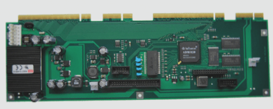
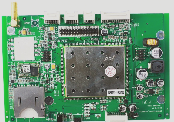
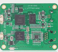
Detection Methods for Assembled PCB Multilayer Circuit Boards
To ensure the quality of PCB multilayer circuit boards, various testing equipment has been developed. The Automatic Optical Inspection (AOI) system is commonly used to inspect inner layers pre-delamination. Post-delamination, the X-ray system ensures alignment accuracy and detects small defects. The scanning laser system inspects the pad layer before reflow soldering. Integrating these systems, along with visual inspection tech on the production line and automated component placement checks, enhances the reliability of the final assembly and soldering of panels.
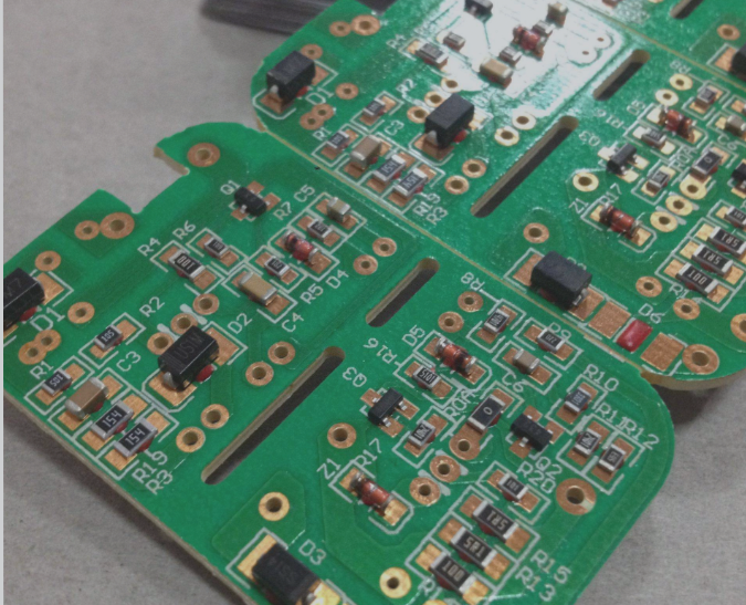
Despite efforts to minimize defects during production, a final inspection of the assembled PCB multilayer circuit board remains crucial. This inspection, the last step in evaluating the product and manufacturing process, can be performed using dynamic methods or automated systems, often combined. “Manual” inspection involves operators visually checking the board for defects, while the automated system uses computer-aided graphical analysis. Automated systems are considered to encompass all detection methods except manual visual inspection.
X-ray technology assesses solder thickness, distribution, internal voids, cracks, desoldering, and presence of solder balls. Ultrasound detects voids, cracks, and unbonded interfaces. AOI evaluates external features like bridging, flux, and component shape. Laser inspection generates 3D images of external features. Infrared detection compares thermal signatures of solder joints to identify faults.
Defects beyond automatic inspection capabilities in assembled PCB multilayer circuit boards are identified. Visual inspection methods should complement automated systems, especially for less common applications. A combo of X-ray and manual optical inspection is most effective for defect detection. Common defects in assembled boards include missing components, component failures, installation errors, poor soldering quality, and solder bridges.
SMT Process Surface Assembly Inspection
The quality and reliability of surface-mount products rely on component manufacturability, reliability, electronic materials, process design, and assembly procedures. To successfully assemble SMT products, strict control of incoming electronic components and materials (incoming inspection) and a DFM review of the SMT process design are essential. Continuous quality checks before and after each stage, including printing, component placement, and soldering, are crucial.
Inspection of the Solder Paste Printing Process
Solder Paste Printing in SMT Process
Solder paste printing is a crucial stage in the Surface Mount Technology (SMT) process, serving as the initial step and significantly impacting the overall quality of the final product. This stage is highly intricate and prone to various defects, with 60%-70% of all defects originating here. To enhance quality control and minimize losses, many SMT lines now incorporate Automatic Optical Inspection (AOI) systems post-printing to detect defects in real time. Common defects include missing solder pads, excessive solder, misalignment, bridging, and more, caused by factors like improper stencil thickness, incorrect printer settings, and poor PCB processing.
Component Placement Process Inspection
The accuracy and efficiency of the component placement process are pivotal for the assembly line’s automation and productivity levels. Real-time monitoring is essential to ensure product quality. Utilizing AOI post-placement helps prevent defective components from progressing to reflow soldering, where they could lead to further issues. Key inspection elements include component placement accuracy, handling of small-pitch devices, pre-reflow defects, PCB surface contamination, and component pin-solder paste contact. Character recognition software aids in identifying placement errors.
Soldering Process Inspection
Post-soldering, a comprehensive inspection is vital to assess product quality. Areas to check include solder joint smoothness, shape correctness, presence of defects like tombstoning and bridging, component misplacement, solder balls, and more. Monitoring PCB surface color changes can also indicate potential defects. Ensuring no short circuits, open circuits, or soldering defects are present is crucial for product integrity.
If you have any inquiries regarding PCBs, feel free to reach out to us at info@wellcircuits.com.