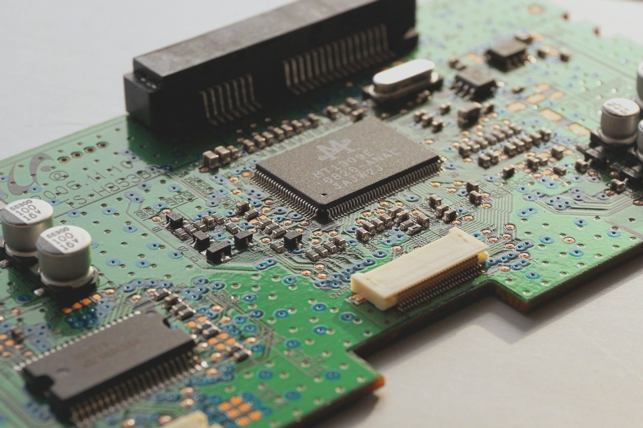
1. **Visual Inspection**
Since the various layers of a PCB are tightly integrated, it is generally difficult to visually determine the number of layers. However, by carefully inspecting the board for faults, it is still possible to make some distinctions. On closer examination, one might notice one or more white insulating layers between the PCB layers. These insulating layers prevent electrical shorts between the different layers. Multi-layer PCBs typically consist of single or double-sided boards with insulating layers placed between each layer and then pressed together. The number of layers in a PCB corresponds to the number of independent wiring layers, and the insulating layers between these layers offer a straightforward way to visually assess the number of PCB layers.
2. **Guide Hole and Blind Hole Alignment Method**
The guide hole method involves using the “guide holes” on the PCB to determine the number of layers. This method leverages the via technology used for circuit connections in multilayer PCBs. To identify how many layers the PCB has, you can examine the via holes.
On the simplest PCB (a single-sided board), components are placed on one side, and wiring is concentrated on the opposite side. To create a multilayer board, holes are drilled so that component pins can pass through to the other side of the board. As a result, guide holes will penetrate the PCB, making the component pins visible and soldered on the opposite side.
For example, on a 4-layer PCB, wiring is routed on the first and fourth layers (signal layers), while the inner layers serve different purposes, such as ground and power layers. The signal layers are placed between the ground and power layers to minimize interference and improve signal integrity. If guide holes are visible on the front side of the PCB but not on the back side, it indicates a 6-layer or 8-layer board. Conversely, if the same via holes are visible on both sides of the PCB, the board is likely a 4-layer design.
However, many PCB manufacturers currently employ a different routing method, where only some of the lines are connected, using buried and blind vias in the process. Blind vias are used to connect several internal layers of the PCB to the surface without passing through the entire board.
Buried vias, on the other hand, only connect the internal layers and are not visible from the surface. Since blind vias do not need to extend through the entire PCB, if the board has six or more layers, it will block light when viewed against a light source. This led to a common saying: distinguishing between four-layer and six-layer (or more) PCBs by whether the vias leak light. While this method has some logic, it is not entirely reliable and should be considered only as a rough guideline.
3. Accumulation Method
Strictly speaking, this is not a formal method but more of an industry insight. However, we consider it to be one of the most accurate ways to judge the number of PCB layers. By analyzing the traces and component placement on a few well-known PCBs, one can often estimate the layer count. This approach works because, in today’s rapidly evolving IT hardware industry, there are only a limited number of PCB manufacturers capable of redesigning complex boards.
For instance, several years ago, many graphics cards, such as the 9550 series, were designed with six-layer PCBs. By carefully comparing the design with newer models, like the 9600PRO or 9600XT, one can observe the differences—mainly the omission of certain components—while maintaining the same overall PCB height.
In the 1990s, a popular belief circulated that the number of PCB layers could be determined by placing the board upright, a claim that many believed to be true. However, this theory was later debunked, as it was physically impossible to discern the layer count with the naked eye, given the limitations of manufacturing technology at the time. This idea evolved into another method: using precision measuring tools like vernier calipers to estimate the number of layers. We disagree with this approach.
Regardless of the measuring tools available, why should we expect a 12-layer PCB to be three times as thick as a 4-layer board? Different PCBs are fabricated using different processes, and there is no universal standard for thickness measurement. Therefore, it is not practical to judge the number of layers based on thickness alone.
In fact, the number of PCB layers significantly influences the design. For example, a minimum of six layers is typically required for dual-CPU installations. This configuration allows for 3 or 4 signal layers, 1 ground layer, and 1 or 2 power layers, ensuring proper signal separation and reduced interference, while providing adequate power supply. In contrast, a 4-layer PCB design is sufficient for most general applications, and a 6-layer design often proves unnecessarily costly without providing substantial performance improvements.
If you have any PCB manufacturing needs, please do not hesitate to contact me.Contact me