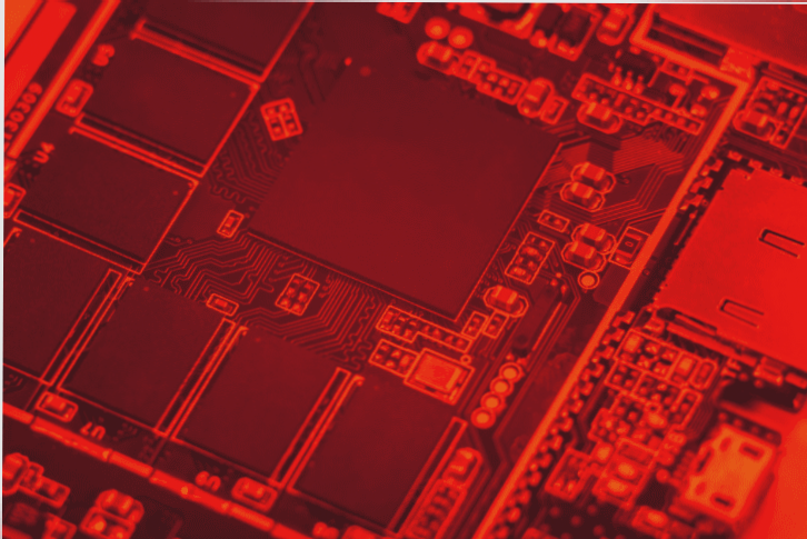
Effective Methods to Reduce Interference on a PCB Board
- Minimize the area of the differential mode signal loop.
- Reduce high-frequency noise return through filtering, isolation, and impedance matching.
- Lower the common mode voltage by implementing proper grounding design.
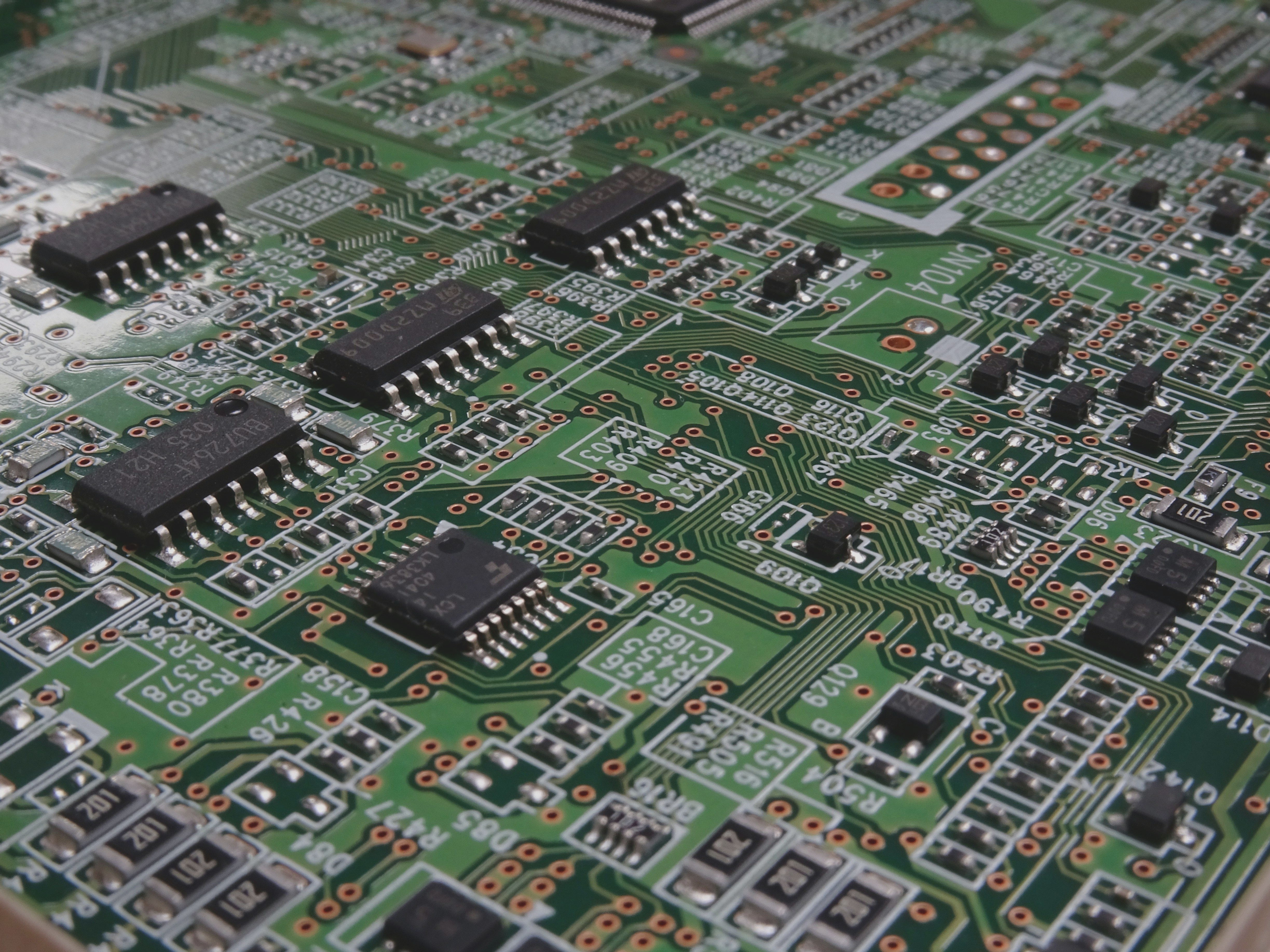
47 Principles of High-Speed PCB EMC Design
Principle 1: Multi-Layer Board Design
If the PCB clock frequency exceeds 5 MHz or the signal rise time is less than 5 ns, a multi-layer board design is generally required. This design helps control the signal loop area effectively.
Principle 2: Key Signal Layers Placement
In multi-layer boards, key signal layers should be positioned adjacent to a complete ground plane to minimize radiation intensity and enhance immunity to interference.
Principle 3: Single-Layer Board Grounding
In single-layer boards, both sides of key signal lines should be covered with ground to prevent crosstalk between signal lines.
Principle 4: Double-Layer Board Layout
In double-layer boards, large ground areas should be placed under key signal lines to reduce the signal loop area.
Principle 5: Power Plane Offset
Offsetting the power plane from its adjacent ground plane helps suppress edge radiation in multi-layer boards.
Principle 6: Layer Alignment
The wiring layer’s projection should align with the reflow plane layer’s area to minimize edge radiation and signal loop area.
Principle 7: Signal Routing
High-frequency signals above 50 MHz should ideally be routed between plane layers in multi-layer boards to minimize radiation.
Principle 8: Grounded Copper Planes
For single-board designs with frequencies above 50 MHz, covering TOP and BOTTOM layers with grounded copper planes helps minimize radiation.
Principle 9: Power Plane Placement
In multilayer PCBs, placing the primary power plane close to the ground plane improves performance by reducing the loop area.
Principle 10: Ground Trace Placement – Single-Layer PCB
In a single-layer PCB, placing a ground trace next to and parallel to the power trace reduces noise and improves signal integrity.
Principle 11: Ground Trace Placement – Double-Layer PCB
In a double-layer PCB, placing a ground trace next to the power trace minimizes noise and maintains signal quality.
Principle 12: Layer Stacks Design
Avoid placing adjacent signal routing layers to prevent crosstalk and maintain signal integrity.
Principle 13: Plane Layers Arrangement
Avoid overlapping projection areas between adjacent plane layers to reduce noise coupling.
Principle 14: Component Alignment
Align components in the direction of signal flow and avoid creating long looping traces to prevent signal degradation.

Principles of PCB Layout for Optimal Performance
-
Separation of Circuit Types
It is crucial to separate digital, analog, and high-speed circuits on the same PCB to minimize interference.
-
Routing Speed-Specific Circuits
High-speed and medium-speed circuits should be routed away from interfaces to prevent noise interference.
-
Placement of Energy Storage Components
Capacitors near high-current devices reduce loop area, enhancing performance.
-
Optimal Location of Power Input Filter
Locating the power input filter circuit near the interface prevents re-coupling of noise signals.
-
Interface Component Placement
Filtering, protection, and isolation components should be placed as close to the interface as possible for optimal performance.
-
Order of Filter and Protection Circuits
When using both filter and protection circuits at the interface, place the protection circuit before the filter to prevent damage from high voltage or current spikes.
If you require PCB manufacturing services, feel free to contact us.