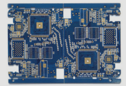
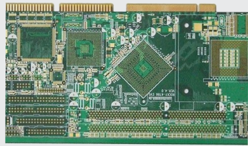
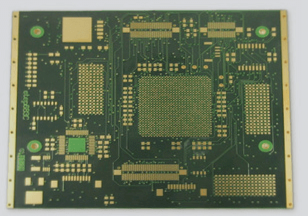
The interconnection of the circuit board system encompasses:
1. Chip-to-board
2. PCB interconnection
3. PCB and external components
In RF design, the electromagnetic characteristics at the interconnection points present significant challenges for engineering design. This article explores various techniques related to the three aforementioned types of interconnection design, including device mounting methods, wiring isolation, and strategies to reduce lead inductance. Currently, there is an observable trend toward increasing frequencies in printed circuit board design. As data rates rise, the bandwidth required for data transmission also elevates, pushing the upper limit of signal frequencies to 1GHz or even higher. While this high-frequency signal technology surpasses the millimeter-wave domain (30GHz), it remains relevant to RF and low-end microwave technologies.
RF engineering design methodologies must effectively address the stronger electromagnetic field effects typically generated in higher frequency bands. These electromagnetic fields can induce signals on adjacent signal lines or PCB traces, leading to undesirable crosstalk (interference and overall noise) that can degrade system performance. Return loss primarily results from impedance mismatch, influencing signals similarly to additive noise and interference.

1. There are two primary negative effects of high return loss:
2. The signal reflected back to the source increases system noise, making it more challenging for the receiver to differentiate between noise and the actual signal.
3. Any reflected signal can significantly degrade signal quality due to alterations in the shape of the input signal.
4. Although digital systems only process binary signals (1s and 0s) and exhibit good fault tolerance, the harmonics generated during high-speed pulse transitions can weaken the signal at higher frequencies.
5. While forward error correction technology can mitigate some negative impacts, it consumes part of the system’s bandwidth for transmitting redundant data, ultimately reducing overall performance.
6. A more effective solution is to leverage RF effects to enhance, rather than detract from, signal integrity. It is advisable for the total return loss of the digital system at its highest frequency (typically the most problematic point) to be -25dB, which corresponds to a VSWR of 1.1.
7. The goal of PCB design is to achieve smaller, faster, and lower-cost solutions. In the context of RF PCBs, high-speed signals can sometimes hinder the miniaturization of PCB designs.
8. The primary method for addressing crosstalk issues is to effectively manage the ground plane, maintain adequate spacing between traces, and reduce lead inductance.
9. The main approach to minimizing return loss is impedance matching. This includes effective management of insulating materials and the isolation of active signal lines from ground lines, particularly between signal lines that are in transition and ground.
10. Since interconnection points represent the weakest links in the circuit chain, the electromagnetic properties at these points present significant challenges in RF design. Each interconnection point must be examined, and any issues must be addressed. The interconnections within a circuit board system comprise three types: between the chip and the circuit board, within the PCB itself, and between the PCB and external devices.
11. First, the interconnection between the chip and the PCB board:
12. Pentium IV and high-speed chips with numerous input/output interconnection points are now available. Regarding the chip itself, its performance is reliable, with processing rates reaching up to 1GHz. The primary issue in connecting the chip to the PCB is the high interconnection density, which can limit the basic structure of the PCB material. A common solution is to utilize local wireless transmitters within the chip to communicate with adjacent circuit boards. Regardless of the effectiveness of this approach, it is clear that in high-frequency applications, IC design technology significantly outpaces PCB design technology.
13. Second, PCB board interconnection:
14. The skills and methods for high-frequency PCB design include:
15. Angling transmission line corners at 45° to reduce return loss;
16. Employing high-performance insulated circuit boards with strictly controlled dielectric constants to effectively manage the electromagnetic field between the insulation and adjacent traces.
17. Avoid using components with leads due to their tap inductance; in high-frequency environments, surface mount components are preferred.
18. For signal vias, avoid the via processing (PTH) method on sensitive boards, as this can introduce lead inductance at the vias. For example, a via connecting layers 1 to 3 on a 20-layer board can adversely affect layers 4 to 19.
19. Ensure a robust ground plane and use molded holes to connect these ground planes, preventing 3D electromagnetic fields from affecting the circuit board.
20. Opt for electroless nickel plating or immersion gold plating processes instead of HASL for electroplating, as these surfaces provide better skin effect for high-frequency currents. Additionally, these highly solderable coatings require fewer leads, helping to reduce environmental impact.
21. The solder mask prevents solder paste flow, but due to thickness variations and unknown insulation properties, a full coating can significantly alter electromagnetic energy in microstrip designs. Generally, a solder dam is used as the solder mask.
22. To enhance PCB design specifications for high-precision etching, ensure that the total error for specified line width is +/-0.0007 inches, manage the undercut and cross-section of trace shapes, and specify the plating conditions for trace side walls. Comprehensive management of trace geometry and surface coatings is crucial for addressing skin effect issues associated with microwave frequencies. If unfamiliar with these methods, consulting an experienced design engineer in military microwave circuit board design is advisable. For instance, a copper-backed coplanar microstrip design may be more cost-effective than a stripline design.
23. Third, PCB and external device interconnection:
24. How can we resolve signal input/output challenges from the circuit board to connections with remote devices? Trompeter Electronics, an innovator in coaxial cable technology, is making strides in this area. Additionally, consider the electromagnetic field illustrated in the accompanying figure. Here, we manage the transition from microstrip to coaxial cable. In coaxial cables, the ground layer is a woven ring, evenly spaced, while in microstrip, the ground plane is beneath the active line. This introduces edge effects that must be understood, predicted, and accounted for during design. Naturally, these mismatches can also lead to return loss, and minimizing this mismatch is essential to avoid noise and signal interference.
25. Managing impedance issues on PCBs is a crucial design consideration. Impedance begins at the board surface, passes through solder joints to connectors, and concludes at the coaxial cable. As impedance varies with frequency, managing it becomes increasingly complex at higher frequencies. Thus, the challenge of using elevated frequencies for broadband signal transmission remains a significant issue in design.
—
1. Chip-to-board
2. PCB interconnection
3. PCB and external components
In RF design, the electromagnetic characteristics at the interconnection points present significant challenges for engineering design. This article explores various techniques related to the three aforementioned types of interconnection design, including device mounting methods, wiring isolation, and strategies to reduce lead inductance. Currently, there is an observable trend toward increasing frequencies in printed circuit board design. As data rates rise, the bandwidth required for data transmission also elevates, pushing the upper limit of signal frequencies to 1GHz or even higher. While this high-frequency signal technology surpasses the millimeter-wave domain (30GHz), it remains relevant to RF and low-end microwave technologies.
RF engineering design methodologies must effectively address the stronger electromagnetic field effects typically generated in higher frequency bands. These electromagnetic fields can induce signals on adjacent signal lines or PCB traces, leading to undesirable crosstalk (interference and overall noise) that can degrade system performance. Return loss primarily results from impedance mismatch, influencing signals similarly to additive noise and interference.
1. There are two primary negative effects of high return loss:
2. The signal reflected back to the source increases system noise, making it more challenging for the receiver to differentiate between noise and the actual signal.
3. Any reflected signal can significantly degrade signal quality due to alterations in the shape of the input signal.
4. Although digital systems only process binary signals (1s and 0s) and exhibit good fault tolerance, the harmonics generated during high-speed pulse transitions can weaken the signal at higher frequencies.
5. While forward error correction technology can mitigate some negative impacts, it consumes part of the system’s bandwidth for transmitting redundant data, ultimately reducing overall performance.
6. A more effective solution is to leverage RF effects to enhance, rather than detract from, signal integrity. It is advisable for the total return loss of the digital system at its highest frequency (typically the most problematic point) to be -25dB, which corresponds to a VSWR of 1.1.
7. The goal of PCB design is to achieve smaller, faster, and lower-cost solutions. In the context of RF PCBs, high-speed signals can sometimes hinder the miniaturization of PCB designs.
8. The primary method for addressing crosstalk issues is to effectively manage the ground plane, maintain adequate spacing between traces, and reduce lead inductance.
9. The main approach to minimizing return loss is impedance matching. This includes effective management of insulating materials and the isolation of active signal lines from ground lines, particularly between signal lines that are in transition and ground.
10. Since interconnection points represent the weakest links in the circuit chain, the electromagnetic properties at these points present significant challenges in RF design. Each interconnection point must be examined, and any issues must be addressed. The interconnections within a circuit board system comprise three types: between the chip and the circuit board, within the PCB itself, and between the PCB and external devices.
11. First, the interconnection between the chip and the PCB board:
12. Pentium IV and high-speed chips with numerous input/output interconnection points are now available. Regarding the chip itself, its performance is reliable, with processing rates reaching up to 1GHz. The primary issue in connecting the chip to the PCB is the high interconnection density, which can limit the basic structure of the PCB material. A common solution is to utilize local wireless transmitters within the chip to communicate with adjacent circuit boards. Regardless of the effectiveness of this approach, it is clear that in high-frequency applications, IC design technology significantly outpaces PCB design technology.
13. Second, PCB board interconnection:
14. The skills and methods for high-frequency PCB design include:
15. Angling transmission line corners at 45° to reduce return loss;
16. Employing high-performance insulated circuit boards with strictly controlled dielectric constants to effectively manage the electromagnetic field between the insulation and adjacent traces.
17. Avoid using components with leads due to their tap inductance; in high-frequency environments, surface mount components are preferred.
18. For signal vias, avoid the via processing (PTH) method on sensitive boards, as this can introduce lead inductance at the vias. For example, a via connecting layers 1 to 3 on a 20-layer board can adversely affect layers 4 to 19.
19. Ensure a robust ground plane and use molded holes to connect these ground planes, preventing 3D electromagnetic fields from affecting the circuit board.
20. Opt for electroless nickel plating or immersion gold plating processes instead of HASL for electroplating, as these surfaces provide better skin effect for high-frequency currents. Additionally, these highly solderable coatings require fewer leads, helping to reduce environmental impact.
21. The solder mask prevents solder paste flow, but due to thickness variations and unknown insulation properties, a full coating can significantly alter electromagnetic energy in microstrip designs. Generally, a solder dam is used as the solder mask.
22. To enhance PCB design specifications for high-precision etching, ensure that the total error for specified line width is +/-0.0007 inches, manage the undercut and cross-section of trace shapes, and specify the plating conditions for trace side walls. Comprehensive management of trace geometry and surface coatings is crucial for addressing skin effect issues associated with microwave frequencies. If unfamiliar with these methods, consulting an experienced design engineer in military microwave circuit board design is advisable. For instance, a copper-backed coplanar microstrip design may be more cost-effective than a stripline design.
23. Third, PCB and external device interconnection:
24. How can we resolve signal input/output challenges from the circuit board to connections with remote devices? Trompeter Electronics, an innovator in coaxial cable technology, is making strides in this area. Additionally, consider the electromagnetic field illustrated in the accompanying figure. Here, we manage the transition from microstrip to coaxial cable. In coaxial cables, the ground layer is a woven ring, evenly spaced, while in microstrip, the ground plane is beneath the active line. This introduces edge effects that must be understood, predicted, and accounted for during design. Naturally, these mismatches can also lead to return loss, and minimizing this mismatch is essential to avoid noise and signal interference.
25. Managing impedance issues on PCBs is a crucial design consideration. Impedance begins at the board surface, passes through solder joints to connectors, and concludes at the coaxial cable. As impedance varies with frequency, managing it becomes increasingly complex at higher frequencies. Thus, the challenge of using elevated frequencies for broadband signal transmission remains a significant issue in design.
—

