1. **Conditioning the Whole Hole**
This term generally refers to the “adjustment” or “modification” of the hole to prepare it for subsequent processes. In a narrower sense, it involves making the walls of the drilled holes “hydrophilic” and “positive” before the PTH (Plated Through Hole) process begins, while simultaneously completing the cleaning steps. This conditioning ensures that the hole walls are properly prepared for the next stages of treatment. The process of preparing the hole walls before the PCB through-hole process is called Hole Conditioning.
2. **Desmearing**
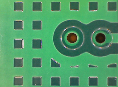
Desmearing refers to the removal of resin smear that occurs during the high friction and heat generated while drilling the PCB. When the temperature exceeds the resin’s Tg (glass transition temperature), the resin softens and can even become fluid, coating the hole walls as the drill bit rotates. Once cooled, the resin forms a hard residue, creating a barrier between the copper in the hole and the copper that will later be deposited on the hole walls. To ensure proper electrical connection in the PTH process, it is essential to remove this smear. If left untreated, the residue will prevent good bonding, as seen in the figure, where an inconsistent gap remains between the copper hole wall and the inner copper ring.
3. **Dichromate Treatment**
(Assuming the sentence for the third point will continue or be expanded as it seems incomplete.)
1. **Cr2O7**
Cr2O7, commonly referred to as K2Cr2O7, (NH4)2Cr2O7, and others, is called “heavy” chromate due to the presence of two chromium atoms in its molecular formula. This type of chromate can be distinguished from other forms of chromate (CrO) by its unique properties.
2. **Etchback**
Etchback refers to a process in multi-layer PCB manufacturing, where the resin and fiberglass substrate between copper ring layers of each through-hole wall are deliberately etched back by approximately 0.5 to 3 mils. This technique is known as “etchback.”
3. **Free Radical**
A “free radical” is a charged particle formed when an atom or molecule loses one or more electrons. Free radicals are highly reactive and can participate in special chemical reactions. For example, the “plasma method” used to remove slag from the hole walls of multi-layer PCBs relies on free radicals. In this process, the board is placed in a sealed chamber filled with O2 and CF4, and high voltage is applied to generate various radicals. These radicals then target the resin portion of the board, effectively removing debris from the holes without affecting the copper.
4. **Negative Etch-back**
In early military-grade or high-reliability multi-layer PCBs, negative etch-back was used to enhance reliability. After cleaning the hole wall for glue residue post-drilling, a further etching process would be applied to each dielectric layer. This would cause the inner copper ring to protrude, forming a more reliable three-bread clip connection after copper plating the hole wall. This process is known as “etch-back.” However, in standard multi-layer PCB production, excessive etching or mistakes during micro-etching (such as over-etching the copper) can result in the shrinking of the inner copper ring, which is known as “anti-etch back.”
5. **Plasma**
Plasma refers to a mixture of “non-polymeric” gases that, when exposed to high-voltage ionization in a vacuum, dissociate into positive and negative ions or free radicals. These particles possess high energy and chemical activity, which makes them distinct from the original gas. Plasma, sometimes referred to as the “fourth state of matter,” exists between the gas and liquid phases and requires continuous energy input to maintain. If energy is removed, plasma quickly neutralizes back into its original mixed gases. The term “plasma” is used due to the high-energy state of the material.
6. **Reverse Etchback**
Reverse etchback occurs when the inner copper ring of a through-hole in a multi-layer PCB is unintentionally etched, causing the inner edge of the ring to recede from the hole wall. As a result, the base material, composed of resin and fiberglass, forms a protrusion. In this case, the inner copper ring diameter becomes larger than the drilled hole diameter. This situation, known as “anti-erosion back,” can result in unreliable interconnections between the inner copper ring and the hole wall. To improve reliability, the base material must be set back, and the copper ring should be deliberately positioned to protrude, creating a more solid connection with the hole wall. This process is called “etchback,” and the reversed outcome is known as “reverse etchback.”
7. **Shadowing**
In the PCB industry, shadowing is used in two distinct contexts. The first relates to infrared (IR) soldering during the assembly of surface-mount devices (SMDs) on a PCB. Here, some components may block infrared radiation, preventing heat from reaching certain areas, resulting in incomplete soldering. This is known as “shadowing.” The second refers to a situation during resin etchback (Etchback) of high-performance multi-layer PCBs, where resin remains in the “dead corners” at the top and bottom of the inner copper ring. These areas are often difficult to clean, and the residual resin can form a shadow, hindering the etchback process.
8. **Swelling Agents**
Swelling agents, or leavening agents, are used after drilling multi-layer PCBs to facilitate the removal of glue residue from the hole walls. The board is immersed in a high-temperature alkaline solution containing organic solvents to soften the glue, making it easier to remove.
9. **Yield**
Yield refers to the percentage of products that pass quality inspection in a production batch. It is a measure of the efficiency and success of the manufacturing process, with a higher yield indicating fewer defects and better overall quality.
If you have any PCB manufacturing needs, please do not hesitate to contact me.Contact me