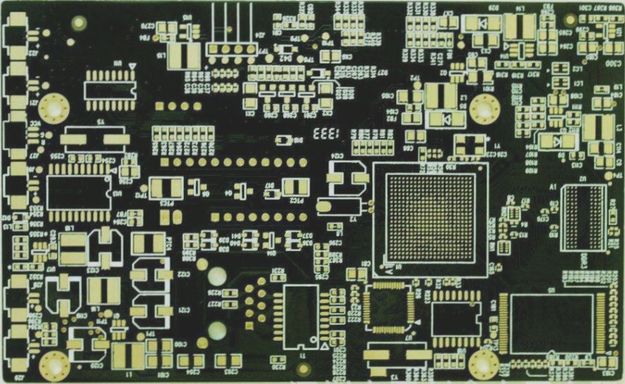
a) How should the layout of printed wires and pads be configured? The line width and spacing are primarily specified in the design drawings. However, our company implements the following adjustments: based on process requirements, we will compensate for the line width and pad ring width. For single-layer boards, we will maximize the pad size to enhance the reliability of customer soldering.
b) When the design line spacing does not meet process requirements (excessively tight spacing may impact performance and manufacturability), we will make adjustments based on pre-design specifications.
c) In general, some PCB manufacturers recommend that for single and double-sided boards, the inner diameter of through holes (VIA) should be set to 0.3mm or larger, the outer diameter to 0.7mm or larger, the line spacing to 8 mils, and the line width to 8 mils or greater. This helps minimize production cycles and reduces manufacturing difficulty.
d) Our smallest drill tool measures 0.3mm, resulting in a finished hole of approximately 0.15mm. The minimum line spacing is 6 mils, and the thinnest line width is also 6 mils. However, this results in a longer manufacturing cycle, which increases costs.

—
2. Line Width Tolerance
The internal control standard for printing line width tolerance is ±15%.
3. Grid Processing
a) To prevent polishing of the copper surface during the wave soldering process and PCB bending from thermal stress post-heating, it is advisable to layout large copper areas in a grid format.
b) The grid spacing should be ≥ 10 mils (minimum 8 mils), with grid line width also at least 10 mils (minimum 8 mils).
4. Thermal Pad Treatment
For extensive grounding areas, the component legs are typically connected to these pads. The design of these connections considers both electrical performance and process requirements; thus, a cross-shaped pad (insulating pad) can be employed to minimize heat dispersion and reduce the risk of virtual solder joints during soldering.
5. Apertures (HOLE)
1. Metallization (PHT) and Non-Metallization (NPTH)
a) Our default specifications are as follows: for non-metallized holes:
When customers set non-metallized properties for mounting holes in the advanced settings of Protel99se (by removing the plating item from the menu), the default is non-metallized holes.
If customers use the holding layer or mechanical 1-layer arc to indicate holes in the design file (without separate holes), the default remains non-metallized.
When NPTH is noted near a hole, we assume the hole is non-metallized.
If customers explicitly request non-metallization (NPTH) in the design notice, we will accommodate their requirements.
b) Component holes, mounting holes, and through holes not mentioned above should be metallized.
2. Aperture Size and Tolerance
a) The PCB component hole in the design pattern, specifically for mounting holes, defaults to the final finished hole size, with an aperture tolerance generally at ±3 mils (0.08 mm).
b) For through holes (i.e., VIA holes), we typically control this with no negative tolerance and a positive tolerance within +3 mils (0.08 mm).
3. Thickness
The average thickness of copper plating in metallized holes is usually no less than 20 μm, with the thinnest areas not dropping below 18 μm.
4. Hole Wall Roughness
The roughness of PTH hole walls is generally maintained at ≤32 μm.
5. Pinhole Problem
a) The positioning pin for our CNC milling machine measures at least 0.9 mm, with the three PIN holes arranged in a triangular pattern.
b) If customers have no special requirements and the design document specifies apertures <0.9 mm, some PCB companies may add PIN holes in suitable locations on the blank wireless road or large copper areas of the board.
—
Let me know if you need any further adjustments!


