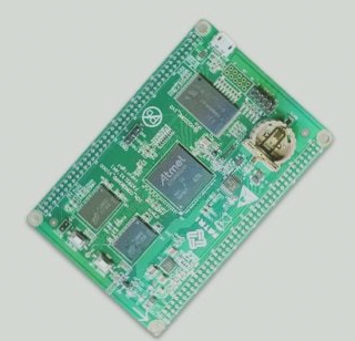
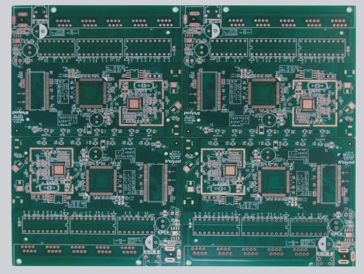
1. Enhance PCB’s anti-deformation ability

The deformation of the circuit board (PCBA board) usually results from the rapid heating and cooling (thermal expansion and contraction) during high-temperature reflow, compounded by uneven distribution of components and copper foil on the circuit board. This unevenness exacerbates the deformation.

Prevent BGA from falling off

To increase the circuit board’s resistance to deformation:

1. Increase the thickness of the PCB. A thickness of 1.6mm or more is recommended. For 0.8mm, 1.0mm, or 1.2mm boards, use furnace fixtures to support and strengthen the board during the reflow process to mitigate deformation.

2. Use high Tg PCB material. High Tg enhances rigidity, though at a higher cost. This involves a trade-off between performance and expense.

3. Add steel bars around the BGA. If space allows, reinforce the BGA with a supporting iron frame to improve its stress resistance.

4. Apply epoxy glue (potted) on the circuit board. Pour glue around the BGA or on the board’s backside to bolster stress resistance.

Second, reduce the deformation of the PCB

Typically, when the circuit board (PCB) is housed in a case, it should be protected. However, with the trend toward thinner, hand-held devices, external forces like bending or impacts can deform the board.

To mitigate deformation from external forces, consider the following:

1. Increase the buffer design in the mechanism. Implement cushioning materials to absorb impacts, ensuring the internal circuit board remains unaffected even if the case deforms. Consider the lifespan and capacity of these buffers.

2. Add screws or positioning and fixing mechanisms around the BGA. If our goal is solely to protect the BGA, we can secure the area near the BGA to prevent deformation in its vicinity.

3. Reinforce the shell to prevent deformation from affecting the internal circuit board.

3. Enhance BGA reliability

1. Apply glue (underfill) to the bottom of the BGA.

2. Increase the size of the BGA solder pads on the circuit board. This will complicate circuit board routing, as the space between solder balls becomes smaller.

3. Utilize SMD (Solder Mask Defined) layout. Cover the solder pads with green solder mask.

4. Employ a Vias-in-Pad (VIP) design. Ensure vias on the solder pads are filled with electroplating to avoid bubble formation during reflow, which could cause solder balls to fracture. This process is akin to reinforcing the ground before building a house.

5. Increase the amount of solder, but ensure it is controlled to avoid short circuits.

6. If working with a finished product, I highly recommend using a [Stress Gauge] to identify stress concentration points on the circuit board. If this is challenging, consider using a computer emulator to determine potential stress concentrations.

Contact

WellCircuits
More than PCB

Upload your GerberFile(7z,rar,zip)