1. Strictly control the length of key network cables
When designing for high-speed transitions, it’s crucial to consider the impact of transmission line effects on PCBs. Modern integrated circuit chips operate at very high clock frequencies, leading to potential issues. Here are some foundational principles to mitigate these problems: for designs using CMOS or TTL circuits with frequencies below 10MHz, keep the wiring under 7 inches. At 50MHz, limit wiring to 1.5 inches; for frequencies of 75MHz or higher, restrict wiring to 1 inch. GaAs chips should not exceed 0.3 inches. Exceeding these limits can result in transmission line problems.
2. Reasonably plan the topology of the wiring
An effective strategy to address high-speed PCB transmission line effects involves choosing appropriate wiring paths and terminal topologies. Wiring topology refers to the sequence and structure of network cable wiring. When employing high-speed logic devices, ensure that branch trace lengths are minimized to prevent distortion of signals with fast edge changes on main signal trunk traces. Typically, PCB routing uses two primary topologies: Daisy Chain routing and Star distribution.

1. For daisy chain wiring, the process starts from the driving end and proceeds to each receiving end sequentially. If a series resistor is used to alter the signal characteristics, it should be positioned close to the driving end. In terms of controlling high-order harmonic interference, daisy chain wiring is highly effective. However, this wiring method has the lowest distribution rate and achieving 100% distribution can be challenging. In practical designs, it’s important to minimize the branch length in daisy chain wiring. The recommended safe length value is: Stub Delay <= Trt * 0.1. For instance, in a high-speed TTL circuit, the branch length should be less than 1.5 inches. This topology occupies less wiring space and can be terminated with a single resistor. Nevertheless, this wiring structure can result in asynchronous signal reception at different receiving ends.
2. The star topology structure can effectively address the asynchronous problem of clock signals, but manually completing the wiring on a high-density PCB board is very challenging. The best approach to accomplish star wiring is by using an automatic router. Each branch requires a terminating resistor, which should match the characteristic impedance of the connection. This impedance can be calculated manually or by using CAD tools to determine the characteristic impedance and the matching resistor value.
3. In the examples above, simple terminal resistors are used. In practice, more complex matching terminals may be employed. One option is the RC matching terminal, which reduces power consumption but is suitable only when the signal is relatively stable. This method is ideal for matching clock line signals. However, the capacitance in the RC matching terminal may affect the shape and propagation speed of the signal.
4. The series resistance matching terminal does not produce additional power consumption but can slow down signal transmission. This method is used for bus drive circuits where time delay is less critical. The advantage of the series resistance matching terminal is that it reduces the number of on-board devices and wiring density.
5. The final method involves using separate matching terminals. In this case, the matching component is placed near the receiving end. This approach prevents signal degradation and minimizes noise effectively. It is typically used for TTL input signals (ACT, HCT, FAST).
6. Additionally, the package type and installation method of the terminal matching resistor must be considered. Generally, SMD surface mount resistors have lower inductance compared to through-hole components, making SMD packages the preferred choice. For in-line resistors, there are two installation options: vertical and horizontal.
7. In vertical installation, one mounting pin of the resistor is very short, which reduces the thermal resistance between the resistor and the circuit board, allowing heat to dissipate more effectively. However, a longer vertical installation increases the resistor’s inductance. Horizontal installation has lower inductance due to its lower profile, but overheating can cause resistance drift. In severe cases, resistance can become an open circuit, leading to PCB trace termination matching failures and potential issues.
8. **3 Methods to Suppress Electromagnetic Interference**
A good signal integrity solution will enhance the electromagnetic compatibility (EMC) of the PCB board. Ensuring a solid grounding is crucial. Using a signal layer with a ground layer is very effective for complex designs. Additionally, minimizing the signal density on the outermost layer of the circuit board is a good way to reduce electromagnetic radiation. This can be achieved by employing the “surface area layer” technology in a “Build-up” PCB design. The surface area layer involves adding a combination of a thin insulating layer and micro-holes to penetrate these layers on a standard process PCB. This setup allows resistance and capacitance to be buried under the surface layer, effectively doubling the trace density per unit area and reducing the PCB size. A smaller PCB area significantly impacts the topological structure of the traces, leading to reduced current loops, shorter branch traces, and lower electromagnetic radiation, which is proportional to the current loop area. Additionally, a smaller PCB size allows the use of high-density lead-foot-packaged devices, further reducing wire length and improving electromagnetic compatibility.
9. **4 Other Available Technologies**
To reduce instantaneous voltage overshoot on the power supply of integrated circuit chips, a decoupling capacitor should be added. This helps effectively mitigate power supply noise and reduce radiation from the power loop on the printed board.
10. Connecting the decoupling capacitor directly to the power pin of the integrated circuit, rather than the power layer, provides the best smoothing effect for noise. This is why some device sockets have decoupling capacitors, and some devices require the decoupling capacitor to be very close to the device.
11. High-speed and high-power devices should be placed together as much as possible to minimize transient overshoot on the power supply voltage. If no power layer is present, long power connections can form a loop between the signal and the loop, becoming a source of radiation and a sensitive circuit.
12. The situation where PCB traces form a loop that does not intersect with the same network cable or other traces is called an open loop. If the loop intersects with other wires in the same network cable, it forms a closed loop. Both scenarios create antenna effects (wire antennas and loop antennas). These antennas generate EMI radiation externally and can also be sensitive circuits themselves. Closed loops are particularly problematic because the radiation they generate is proportional to the area of the loop.
When designing for high-speed transitions, it’s crucial to consider the impact of transmission line effects on PCBs. Modern integrated circuit chips operate at very high clock frequencies, leading to potential issues. Here are some foundational principles to mitigate these problems: for designs using CMOS or TTL circuits with frequencies below 10MHz, keep the wiring under 7 inches. At 50MHz, limit wiring to 1.5 inches; for frequencies of 75MHz or higher, restrict wiring to 1 inch. GaAs chips should not exceed 0.3 inches. Exceeding these limits can result in transmission line problems.
2. Reasonably plan the topology of the wiring
An effective strategy to address high-speed PCB transmission line effects involves choosing appropriate wiring paths and terminal topologies. Wiring topology refers to the sequence and structure of network cable wiring. When employing high-speed logic devices, ensure that branch trace lengths are minimized to prevent distortion of signals with fast edge changes on main signal trunk traces. Typically, PCB routing uses two primary topologies: Daisy Chain routing and Star distribution.
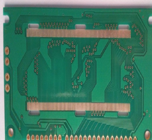
1. For daisy chain wiring, the process starts from the driving end and proceeds to each receiving end sequentially. If a series resistor is used to alter the signal characteristics, it should be positioned close to the driving end. In terms of controlling high-order harmonic interference, daisy chain wiring is highly effective. However, this wiring method has the lowest distribution rate and achieving 100% distribution can be challenging. In practical designs, it’s important to minimize the branch length in daisy chain wiring. The recommended safe length value is: Stub Delay <= Trt * 0.1. For instance, in a high-speed TTL circuit, the branch length should be less than 1.5 inches. This topology occupies less wiring space and can be terminated with a single resistor. Nevertheless, this wiring structure can result in asynchronous signal reception at different receiving ends.
2. The star topology structure can effectively address the asynchronous problem of clock signals, but manually completing the wiring on a high-density PCB board is very challenging. The best approach to accomplish star wiring is by using an automatic router. Each branch requires a terminating resistor, which should match the characteristic impedance of the connection. This impedance can be calculated manually or by using CAD tools to determine the characteristic impedance and the matching resistor value.
3. In the examples above, simple terminal resistors are used. In practice, more complex matching terminals may be employed. One option is the RC matching terminal, which reduces power consumption but is suitable only when the signal is relatively stable. This method is ideal for matching clock line signals. However, the capacitance in the RC matching terminal may affect the shape and propagation speed of the signal.
4. The series resistance matching terminal does not produce additional power consumption but can slow down signal transmission. This method is used for bus drive circuits where time delay is less critical. The advantage of the series resistance matching terminal is that it reduces the number of on-board devices and wiring density.
5. The final method involves using separate matching terminals. In this case, the matching component is placed near the receiving end. This approach prevents signal degradation and minimizes noise effectively. It is typically used for TTL input signals (ACT, HCT, FAST).
6. Additionally, the package type and installation method of the terminal matching resistor must be considered. Generally, SMD surface mount resistors have lower inductance compared to through-hole components, making SMD packages the preferred choice. For in-line resistors, there are two installation options: vertical and horizontal.
7. In vertical installation, one mounting pin of the resistor is very short, which reduces the thermal resistance between the resistor and the circuit board, allowing heat to dissipate more effectively. However, a longer vertical installation increases the resistor’s inductance. Horizontal installation has lower inductance due to its lower profile, but overheating can cause resistance drift. In severe cases, resistance can become an open circuit, leading to PCB trace termination matching failures and potential issues.
8. **3 Methods to Suppress Electromagnetic Interference**
A good signal integrity solution will enhance the electromagnetic compatibility (EMC) of the PCB board. Ensuring a solid grounding is crucial. Using a signal layer with a ground layer is very effective for complex designs. Additionally, minimizing the signal density on the outermost layer of the circuit board is a good way to reduce electromagnetic radiation. This can be achieved by employing the “surface area layer” technology in a “Build-up” PCB design. The surface area layer involves adding a combination of a thin insulating layer and micro-holes to penetrate these layers on a standard process PCB. This setup allows resistance and capacitance to be buried under the surface layer, effectively doubling the trace density per unit area and reducing the PCB size. A smaller PCB area significantly impacts the topological structure of the traces, leading to reduced current loops, shorter branch traces, and lower electromagnetic radiation, which is proportional to the current loop area. Additionally, a smaller PCB size allows the use of high-density lead-foot-packaged devices, further reducing wire length and improving electromagnetic compatibility.
9. **4 Other Available Technologies**
To reduce instantaneous voltage overshoot on the power supply of integrated circuit chips, a decoupling capacitor should be added. This helps effectively mitigate power supply noise and reduce radiation from the power loop on the printed board.
10. Connecting the decoupling capacitor directly to the power pin of the integrated circuit, rather than the power layer, provides the best smoothing effect for noise. This is why some device sockets have decoupling capacitors, and some devices require the decoupling capacitor to be very close to the device.
11. High-speed and high-power devices should be placed together as much as possible to minimize transient overshoot on the power supply voltage. If no power layer is present, long power connections can form a loop between the signal and the loop, becoming a source of radiation and a sensitive circuit.
12. The situation where PCB traces form a loop that does not intersect with the same network cable or other traces is called an open loop. If the loop intersects with other wires in the same network cable, it forms a closed loop. Both scenarios create antenna effects (wire antennas and loop antennas). These antennas generate EMI radiation externally and can also be sensitive circuits themselves. Closed loops are particularly problematic because the radiation they generate is proportional to the area of the loop.

