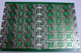
1. Recently, our PCB company has encountered issues with a phenomenon known as “micro short circuit inside the circuit board.” After extensive investigation, we have finally made some breakthroughs in understanding this issue. We discovered instances of micro short circuits in the circuit boards. Following analysis with the PCB manufacturing facility, we traced the defects primarily to [CAF (Conductive Anodic Filament)], also referred to as [Glass Fiber Leakage]. This revelation is significant, as customers were becoming frustrated with our inability to identify the problem.

2. Identifying the CAF issue is quite challenging. First, it’s crucial to pinpoint the location of the short circuit on the circuit board. Next, all potential lines need to be cut to gradually narrow down the possible areas of the short circuit. Ideally, this should be done by examining connections between vias, traces, or even measuring which layer of copper foil is involved in the short circuit. This thorough approach increases the chances of finding evidence of a micro short circuit.

3. If you’re not yet familiar with what CAF entails, I recommend reviewing this article first.

4. During this investigation, we engaged two laboratories, [X Special] and [XX Institute], for cross-section analysis. [X Special] reported no issues, while [XX Institute] suggested that gaps in the glass fiber cloth might lead to CAF. However, since the defective circuit boards sampled varied and the micro short circuit phenomenon was not consistently present, it remains unclear which laboratory’s findings are correct.

Later, after obtaining the actual micro-short circuit board, we dispatched an engineer to the PCB factory with the board and requested an on-site slice analysis. This time, it was confirmed that the CAF phenomenon was indeed present. However, the board manufacturer attributes the CAF issue to the proximity of the through holes (PTH vias) and blind vias. They are now reconsidering the initially recommended distance of 0.4mm, increasing it to at least 0.5mm. The gap from the edge of the hole to the drilling point is currently as small as 0.1mm, but requesting a distance of 0.5mm retroactively is both critical and irresponsible.

We confidently informed the manufacturer that during their review of the PCB, they did not raise any concerns regarding the hole-to-hole distance. The project board factory should have more experience than our system factory, even if the design is somewhat risky. Nevertheless, the board factory must still bear significant responsibility. While we did not demand compensation, we requested that they propose improvement measures and preventive actions.

Below are the improvement measures suggested by the board factory to address the CAF issue:

1. **Change in PP Filling Material Design**: The PP filling material has been changed from S1000 to S1000H, as the board factory indicated that S1000H exhibits better resistance to CAF.

2. **Modification of PP Stacking Structure and Ratio**: The core PP has been reduced from the original 5 sheets of 7628 to 4 sheets, and high RC fillers have been introduced. To compensate for the reduced thickness of the Core’s PP, a layer of 3313 has been added to both the upper and lower PP layers to maintain the original thickness of the base material.

However, we encountered issues during the gold processing; we used EDX to analyze Au instead of Cu. The board utilized by our company employs an ENIG finish.

▼ The image below shows a report from the laboratory section, revealing cracks in the glass fiber cloth. Some conductive substances are seen penetrating and growing along the gaps of the glass fiber bundles, although a short circuit has not yet occurred.

▼ When suspecting the presence of CAF in the PCB, initial steps should include electrical measurement and circuit cutting to gradually narrow down the CAF’s scope. It may be necessary to remove electronic components from the board to eliminate potential interference.

▼ As we gradually pinpoint the location of CAF, we can collaborate with Gerber to assess whether the PCB structure has issues related to overly close through holes or traces.

▼ The image below displays the appearance of the sliced board after confirming that the short circuit continues. Before applying a chemical solution, a long strip of “copper” can be observed across both the through hole and the blind hole. However, this could also be attributed to copper from the wall of the through hole being transferred during slicing and grinding.

The image depicts the slice of the board after confirming that the short circuit persists. Before chemical treatment, a long strip of the same element spans across the through hole and the blind hole. However, it may also be due to copper from the wall of the through hole being inadvertently brought over during slicing and grinding.

ACF (Conductive Anodic Filament) is associated with the leakage phenomenon of conductive pad filaments. The image shows the treated slices, cleaned of possible contaminants from grinding. EDX analysis revealed the presence of Au (gold) between the through hole and the blind hole.

▼ The Au (gold) element identified by EDX is located at the first position between the through hole and the blind hole.

ACF (Conductive Anodic Filament) relates to the leakage phenomenon of conductive pad filaments. Using EDX, the Au (gold) element was found at the first position between the through hole and the blind hole.
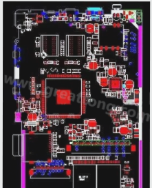
▼ The Au (gold) element identified by EDX is situated at the second position between the through hole and the blind hole.
ACF (Conductive Anodic Filament) is linked to the leakage phenomenon of conductive pad filaments. Using EDX, the Au (gold) element is identified at the second position between the through hole and the blind hole.

Contact

WellCircuits
More than PCB

Upload your GerberFile(7z,rar,zip)