In PCB design, we continually seek new technical advancements to streamline our processes and achieve greater efficiency, particularly as designs become increasingly compact and intricate. Among these innovations is the microvia, a laser-drilled through-hole that is smaller and boasts distinct aspect ratios compared to conventional through-holes. Due to their diminutive size, microvias simplify the task of routing wiring trajectories, enabling us to densely pack more wiring into tighter spaces. Here’s a detailed exploration of microvia aspect ratios and their utility in PCB design.
Let’s begin by understanding some fundamental aspects of through-holes and their applications in printed circuit boards (PCBs). Through-holes are apertures drilled into PCBs, serving to transmit electrical signals from one layer to another. Analogous to how wiring facilitates horizontal signal transmission on a PCB, through-holes facilitate vertical signal transmission. These apertures vary in size, ranging from small to large, with larger through-holes typically employed for power supply, grounding, and mechanical connections to the board. Conventional through-holes are fashioned through mechanical drilling and can be categorized as follows:
1. Through-hole: Drilled from the top surface to the bottom of the PCB.
2. Blind hole: Drilled from the outer surface to an inner layer of the circuit board without traversing the entire board.
3. Buried hole: Commences and concludes within inner layers of the board, without extending to any outer layers.
In contrast, microthrough-holes, as their name suggests, deviate from standard through-holes by being laser-drilled, resulting in smaller dimensions. Typically, mechanical holes are no less than 0.006 inches (0.15 mm) in width, beyond which microvias come into play. Microvias typically span only two layers, as plating copper into these tiny holes poses challenges for manufacturers. For applications necessitating connectivity across more than two layers, microvias can be stacked atop one another.
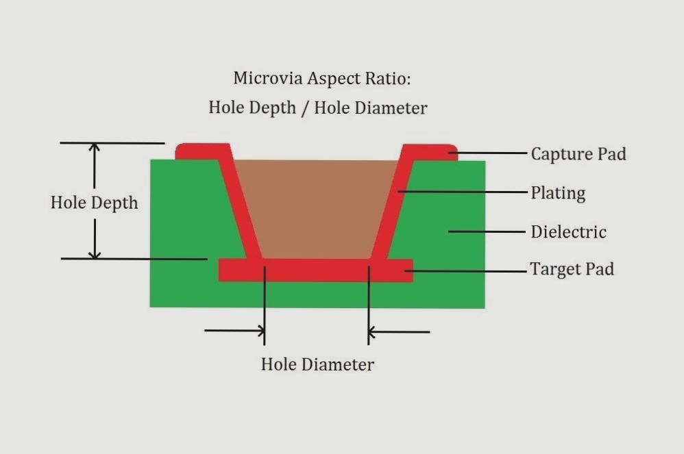
Microvias originating from the surface layer do not require filling, whereas buried microvias are filled with various materials based on their intended application. Stacked microvias are commonly filled with electroplated copper to facilitate interconnection between stacked through-holes. Alternatively, microvias can be interconnected and bridged with short wires, as illustrated below, showcasing a distinct profile compared to conventional through-holes, resulting in disparate aspect ratios.

1. The aspect ratio of a through-hole is the ratio of the depth of the hole to the diameter of the hole (hole depth to hole diameter). For example, a standard circuit board that is 0.062” thick and has 0.020” through holes should have an aspect ratio of 3:1. This ratio serves as a guide to ensure that manufacturers do not exceed their capabilities with the equipment they use for drilling. For standard boreholes, the aspect ratio should normally not exceed 10:1, which will allow a 0.062-inch board to drill 0.006 inch (0.15 mm) through it.
2. When using microholes, the aspect ratio varies greatly depending on their size and depth. Electroplating smaller holes can be difficult, and trying to electroplate a single hole on 10 layers of a board causes many problems for PCB manufacturers. However, if the holes span only two of these layers, plating becomes much easier. The IPC used to define microvias based on their size, which was 0.006 in. (0.15 mm) or less. Over time, this size became so common that IPC decided to change its definition to avoid constantly updating its specifications as technology changed. Today, IPC defines a microhole as a hole with an aspect ratio of 1:1, as long as the hole is no deeper than 0.010 inch or 0.25 mm.
3. In PCB design, the aim is to achieve more routing in a smaller area as the density of PCB technology increases. This has led to the use of blind and buried through holes, as well as the method of embedding through holes in surface-mounted pads. However, because of the additional drilling steps involved, blind and buried through holes are more difficult to manufacture, and drilling can leave material in the hole, leading to manufacturing defects. Conventional through-holes are also often too large to fit into the smaller surface-mount pads found in today’s high-density devices. However, microvias can help solve all of these problems:
4. – MICROVIA makes it easier to manufacture small blind and buried holes.
– The micro-through-holes will be suitable for smaller surface-mounted pads, making them particularly suitable for high-pin count devices such as ball-grid arrays (BGA).
– Due to their small size, microvias allow more wiring to be done around them.
– Due to their size, microvias can also help reduce EMI and improve other signal integrity issues.
5. Microvias are an advanced method of PCB manufacturing, and if your board does not require them, you will obviously want to use standard holes to reduce costs. However, if your design is dense and requires extra space, check to see if using microvias can help. As always, it is a good idea to consult with the contract manufacturer before designing a PCB with microholes.
6. Once you have established contact with the manufacturer, the next step is to configure your PCB design tools to use microholes. To effectively incorporate the details of a microhole design, several adjustments need to be made in the tool. This will include implementing new through-hole shapes and corresponding design rules. Microvias can be stacked, a feature often unavailable with regular through-holes, so your tool must be able to handle this as well.
Let’s begin by understanding some fundamental aspects of through-holes and their applications in printed circuit boards (PCBs). Through-holes are apertures drilled into PCBs, serving to transmit electrical signals from one layer to another. Analogous to how wiring facilitates horizontal signal transmission on a PCB, through-holes facilitate vertical signal transmission. These apertures vary in size, ranging from small to large, with larger through-holes typically employed for power supply, grounding, and mechanical connections to the board. Conventional through-holes are fashioned through mechanical drilling and can be categorized as follows:
1. Through-hole: Drilled from the top surface to the bottom of the PCB.
2. Blind hole: Drilled from the outer surface to an inner layer of the circuit board without traversing the entire board.
3. Buried hole: Commences and concludes within inner layers of the board, without extending to any outer layers.
In contrast, microthrough-holes, as their name suggests, deviate from standard through-holes by being laser-drilled, resulting in smaller dimensions. Typically, mechanical holes are no less than 0.006 inches (0.15 mm) in width, beyond which microvias come into play. Microvias typically span only two layers, as plating copper into these tiny holes poses challenges for manufacturers. For applications necessitating connectivity across more than two layers, microvias can be stacked atop one another.
Microvias originating from the surface layer do not require filling, whereas buried microvias are filled with various materials based on their intended application. Stacked microvias are commonly filled with electroplated copper to facilitate interconnection between stacked through-holes. Alternatively, microvias can be interconnected and bridged with short wires, as illustrated below, showcasing a distinct profile compared to conventional through-holes, resulting in disparate aspect ratios.

1. The aspect ratio of a through-hole is the ratio of the depth of the hole to the diameter of the hole (hole depth to hole diameter). For example, a standard circuit board that is 0.062” thick and has 0.020” through holes should have an aspect ratio of 3:1. This ratio serves as a guide to ensure that manufacturers do not exceed their capabilities with the equipment they use for drilling. For standard boreholes, the aspect ratio should normally not exceed 10:1, which will allow a 0.062-inch board to drill 0.006 inch (0.15 mm) through it.
2. When using microholes, the aspect ratio varies greatly depending on their size and depth. Electroplating smaller holes can be difficult, and trying to electroplate a single hole on 10 layers of a board causes many problems for PCB manufacturers. However, if the holes span only two of these layers, plating becomes much easier. The IPC used to define microvias based on their size, which was 0.006 in. (0.15 mm) or less. Over time, this size became so common that IPC decided to change its definition to avoid constantly updating its specifications as technology changed. Today, IPC defines a microhole as a hole with an aspect ratio of 1:1, as long as the hole is no deeper than 0.010 inch or 0.25 mm.
3. In PCB design, the aim is to achieve more routing in a smaller area as the density of PCB technology increases. This has led to the use of blind and buried through holes, as well as the method of embedding through holes in surface-mounted pads. However, because of the additional drilling steps involved, blind and buried through holes are more difficult to manufacture, and drilling can leave material in the hole, leading to manufacturing defects. Conventional through-holes are also often too large to fit into the smaller surface-mount pads found in today’s high-density devices. However, microvias can help solve all of these problems:
4. – MICROVIA makes it easier to manufacture small blind and buried holes.
– The micro-through-holes will be suitable for smaller surface-mounted pads, making them particularly suitable for high-pin count devices such as ball-grid arrays (BGA).
– Due to their small size, microvias allow more wiring to be done around them.
– Due to their size, microvias can also help reduce EMI and improve other signal integrity issues.
5. Microvias are an advanced method of PCB manufacturing, and if your board does not require them, you will obviously want to use standard holes to reduce costs. However, if your design is dense and requires extra space, check to see if using microvias can help. As always, it is a good idea to consult with the contract manufacturer before designing a PCB with microholes.
6. Once you have established contact with the manufacturer, the next step is to configure your PCB design tools to use microholes. To effectively incorporate the details of a microhole design, several adjustments need to be made in the tool. This will include implementing new through-hole shapes and corresponding design rules. Microvias can be stacked, a feature often unavailable with regular through-holes, so your tool must be able to handle this as well.

