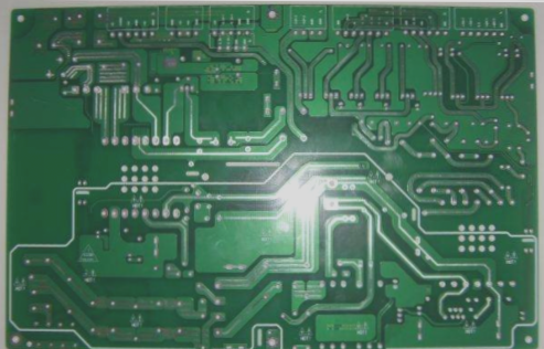
Understanding Electromagnetic Interference (EMI) in PCB Design
Electronic engineers often face the challenge of dealing with Electromagnetic Interference (EMI) in high-speed devices. EMI can lead to signal disruptions and impact the safety and reliability of electronic systems. To address EMI concerns, it is crucial to carefully plan the PCB layout.
Definition of Electromagnetic Interference (EMI)
Electromagnetic Interference (EMI) can be categorized into radiated interference and conducted interference. Radiated interference disrupts signals through space, while conducted interference transmits interference through conductive media. In PCB design, sources of radiated interference include integrated circuit pins and high-frequency signal traces.
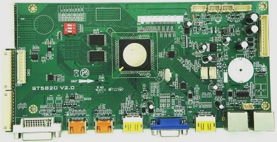
Effective PCB Design Techniques for EMI Reduction
- Common Mode EMI Interference Source: Using low-value inductors and minimizing trace lengths can help reduce common-mode EMI.
- Reducing Loop Area: Minimizing loop areas and utilizing power planes can mitigate EMI effects.
- Filtering: Decoupling capacitors, EMI filters, and magnetic components can suppress unwanted interference.
- Electromagnetic Shielding: Placing signal traces close to power or ground layers enhances shielding effectiveness.
- Component Layout: Organizing components by function and isolating digital and analog circuits can reduce susceptibility to interference.
- Routing Considerations: Proper routing, wide power traces, and minimizing vias help prevent signal interference.
- Increasing PCB Dielectric Constant / Thickness: Adjusting dielectric properties can impact EMI performance.
By implementing these PCB design techniques, engineers can effectively reduce Electromagnetic Interference (EMI) and enhance the overall electromagnetic compatibility of electronic systems.
Preventing PCB Radiation: Tips for High-Frequency Components
Enhancing the dielectric constant of your PCB is crucial in containing high-frequency components like transmission lines to prevent outward radiation. Moreover, adjusting the PCB thickness and microstrip line thickness can effectively minimize electromagnetic leakage and further decrease radiation levels.
Latest PCB Manufacturing Updates:
- Advanced Materials: Explore new dielectric materials with higher permittivity for improved performance.
- Miniaturization Techniques: Learn about cutting-edge methods for reducing microstrip line thickness without compromising quality.
- EMI Shielding Solutions: Discover innovative shielding technologies to enhance PCB radiation protection.
If you require professional PCB manufacturing services or have any inquiries, feel free to reach out to us.