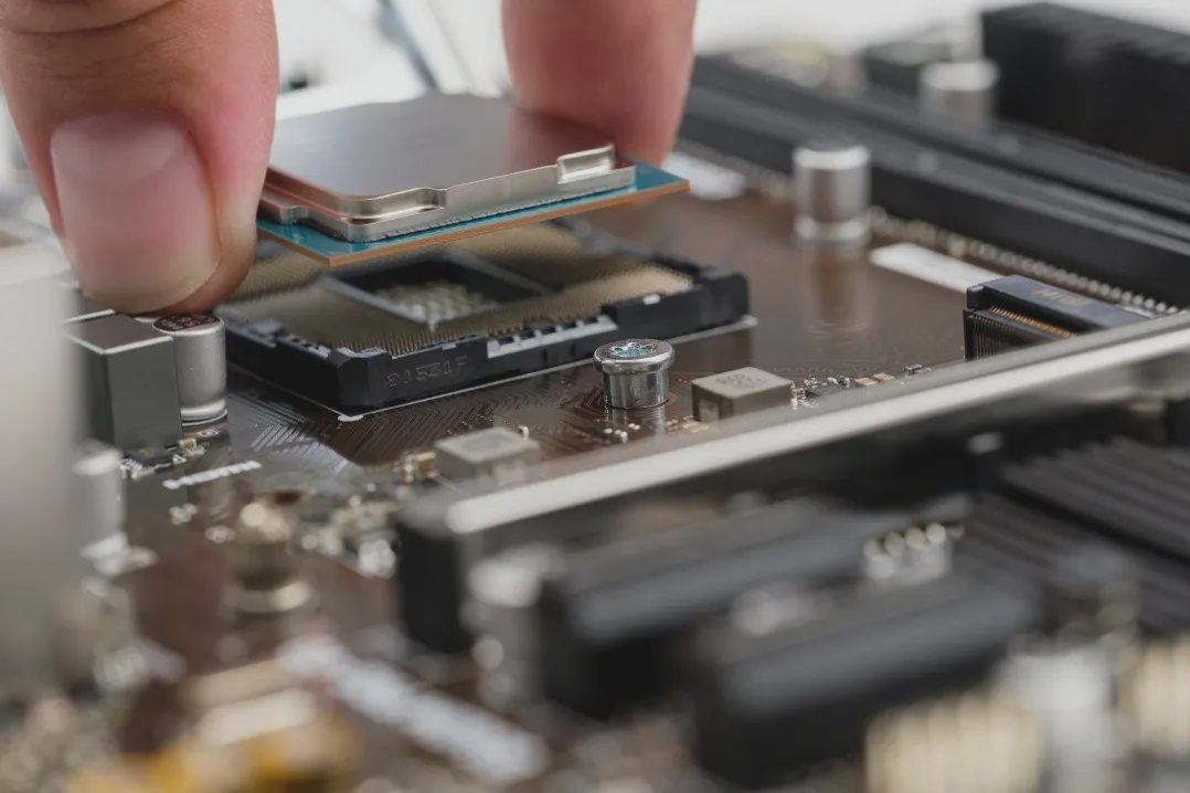
Strategies to Improve PCB Stress Resistance
-
1. Minimize Temperature Impact
Controlling temperature fluctuations during PCB fabrication is crucial to reduce stress. Lowering reflow oven temperatures and managing heating/cooling rates can mitigate plate bending and warpage. However, be cautious of potential solder short circuits.
-
2. Opt for High Tg Materials
Utilize materials with a higher Glass Transition Temperature (Tg) to enhance stress and deformation resistance. Lower Tg materials soften quicker in the reflow oven, increasing the risk of deformation.
-
3. Increase Board Thickness
Consider using thicker circuit boards (e.g., 1.6mm) to maintain post-reflow integrity and reduce the chances of bending and deformation, especially for non-critical weight and size requirements.
-
4. Optimize Board Size and Panel Number
Reduce PCB size and minimize panel numbers to prevent issues like denting and deformation during the reflow process. Aligning boards along the reflow furnace chain’s edge and passing through using the narrow edge can help minimize deformation.
-
5. Implement Furnace Tray Fixtures
Utilize reflow carriers or templates to stabilize PCBs during thermal expansion and contraction, reducing deformation risks. Adding covers to clamp boards between upper and lower pallets can further decrease deformation during reflow.
-
6. Prefer Routing Over V-Cut for Sub-Boards
Avoid V-Cutting for sub-boards as it can compromise structural integrity. If V-Cutting is necessary, minimize the depth to maintain board strength.