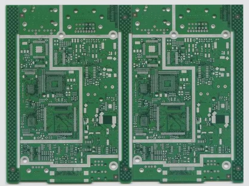
**Causes and Solutions of PCB Technology Negative Film Deformation**
**Reasons:**
(1) Poor temperature and humidity control.
(2) Excessive temperature in the exposure machine.
**Solutions:**
(1) Maintain temperature at 22±2°C and humidity at 55%±5% RH.
(2) Utilize a cold light source or an aerator with a cooling device, and regularly replace the spare film.
**PCB Technology’s Negative Film Deformation Solution**
**Negative Film Distortion Correction Process:**
1. **Change the Hole Position Method:**
Master the operation of the digital programmer. First, compare the negative film with the drilled test board, and measure the deformation in both length and width.
1. On the digital programmer, adjust the hole position according to the deformation by extending or shortening it. Use a drilled test board with these adjusted holes to match the deformed negative film. This method eliminates the tedious work of splicing films and ensures both the completeness and accuracy of the graphics.
2. Hanging method: To account for changes in the negative film due to environmental temperature and humidity, place the film in a sealed bag and hang it for 4-8 hours under working conditions before copying. This pre-deformation ensures minimal distortion after copying.
3. Splicing method: For patterns with simple lines, wide line widths, large spacing, and irregular deformation, cut the deformed part of the negative film and re-splice it onto the drilled test board holes before copying.
4. PCB pad overlap method: Expand the hole on the test board to the pad size and remove the deformed line segment to meet the minimum loop width technical requirements.
5. Texture method: Proportionally enlarge the graphics on the deformed film and then reposition the printing plate.
6. Shooting method: Use a camera to zoom in or out on the deformed image.
**Notes on these related methods**
1. Splicing method:
– Application: Suitable for less dense coating film lines and inconsistent deformation across layers; ideal for solder mask and multi-layer power grounding film.
– Not applicable: High wire density films with line widths and spacings less than 0.2mm.
– Note: Minimize damage to wires and avoid damaging the gasket. Ensure correct connection during splicing and copying.
2. Changing the hole position:
– Application: Suitable for uniformly deformed layers and high-density negatives.
– Not applicable: When the film deforms unevenly or exhibits severe local deformation.
– Note: After adjusting hole positions with the programmer, reset the tolerance hole positions.
3. Hanging method:
– Applicable: For films that have not been deformed and are prevented from deforming after copying.
– Not applicable: For already deformed negatives.
– Note: Dry the film in a ventilated, dark environment to avoid contamination and match the air temperature to the workplace conditions.
4. Pad overlap method:
– Applicable: For less dense graphics with line widths and spacings greater than 0.30mm.
– Not applicable: For users with strict appearance requirements for printed circuit boards.
– Note: Overlapping can lead to oval-shaped PCB pads and deformation along the pad’s edge.
5. Shooting method:
– Application: Effective when the PCB film deforms uniformly in both length and width directions. Use silver salt film if bulky drilling test boards are impractical.
– Not applicable: When the film deforms differently in length and width directions.
– Note: Ensure precise focus to avoid line distortion and be prepared for multiple adjustments to achieve a satisfactory circuit pattern.