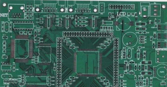
Electromagnetic Compatibility (EMC) in PCB Design
Electromagnetic compatibility (EMC) is crucial for electronic equipment to function effectively in various electromagnetic environments. The goal of EMC design is to equip devices with the ability to handle external interferences and minimize electromagnetic interference emitted to other devices.
Key Strategies for EMC Design:
- Optimal Wire Width Selection: Choose shorter and wider wires to reduce inductance and suppress interference. Clock traces and signal lines carrying transient currents should be kept short, with wire widths of 1.5mm for discrete components and 0.2 to 1.0 mm for integrated circuits.
- Employing Appropriate Wiring Strategies: Utilize equal wiring to reduce inductance or consider a mesh wiring structure for optimal layout. Routing horizontally on one side and vertically on the other side of the board can help minimize interference.
- Suppression of Crosstalk: Avoid prolonged and equidistant wiring to reduce crosstalk. Maximize spacing between wires and incorporate grounded traces between sensitive signal lines to suppress interference effectively.
By implementing these strategies, PCB designers can enhance the electromagnetic compatibility of electronic devices, ensuring reliable operation in diverse electromagnetic environments.

