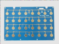
Moisture-proof Insulation for PCB Circuit Boards
A PCB, or printed circuit board, is a critical component in electronic systems. Flexible PCBs, made from materials like imide or polyester film, offer high wiring density, light weight, thin thickness, and excellent bending properties. These boards can be rigid or flexible, combining the advantages of both types.
Moisture-proof insulation is essential for PCBs during assembly and operation. Specialized moisture-proof insulating UV glue is used for this purpose.
Applying Moisture-proof Insulating UV Glue on PCBs
- Best Method: Apply the glue directly with a brush or by hand. Adjust the consistency with a thinner if needed.
- Spraying Process:
- Dilute CRCBOND UV773 with a specific thinner for spraying.
- Transfer the adhesive to a spray pot and apply it by spraying.
- Clean the spray pot after use.
- Soaking Process:
- Immerse the diluted adhesive into a soaking bucket, ensuring a gradual immersion to prevent air bubbles.
- Drying time ranges from 2 to 10 minutes; avoid heating and drying.
- Remove any hard skin formed on the adhesive surface before reuse.
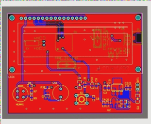
PCB Design: Via and Copper Connections
In PCB design, following design rules is crucial for project success. Clear rule definitions help designers in layout and routing, ensuring high-quality designs. Compliance with electrical, routing, plane, and other rules is essential. Rule-based techniques for PCB copper design involve modifying connections and eliminating cross-shaped connections in Altium Designer.
PCB Design and Manufacturing: Managing Copper Edge Constraints
When designing and manufacturing PCBs, engineers often face mechanical constraints that require them to keep large copper areas within a certain distance from the board’s edge. This is crucial to prevent issues like roller edge problems and electrical shorts caused by copper exposure at the edges.
One common approach to address this issue is by creating a reserved layer at the edge of the board and adjusting the distance between the copper and this reserved layer. By setting different safety distances for copper pouring, engineers can effectively reduce the copper edge while ensuring the integrity of the circuit board.
- For example, setting the safety distance for the entire board at 10 mils and the safety distance for copper pouring at 20 mils can help reduce the copper edge by 20 mils.
- This method not only enhances the board’s overall reliability but also helps eliminate excess copper in the device area, contributing to better performance.
Utilizing query statements in the design process can further streamline the management of copper objects, offering engineers a more precise and efficient way to optimize copper placement on the PCB.