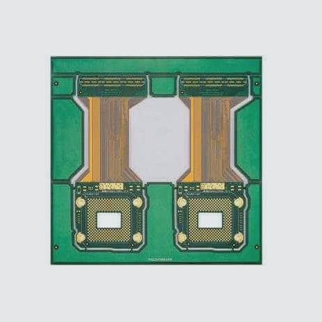
Multilayer Circuit Board Stack Structure
When designing a multilayer circuit board, it is crucial to consider the size of the circuit, PCB dimensions, and electromagnetic compatibility (EMC) requirements. This helps in determining the suitable board structure, whether it is a 4-layer, 6-layer, or higher layer count PCB.
The positioning of inner layers and allocation of signals across these layers play a significant role in defining the multilayer PCB stack structure. This structure is essential for EMC performance and mitigating electromagnetic interference.
Latest Information on Multilayer Circuit Board Stack Structures:
- Choosing the right layer count is crucial for optimal performance.
- Factors like wiring capabilities, manufacturing costs, and complexity influence the decision.
- EDA tools are used to analyze wiring density and configure special wiring setups.
- Considerations for signal lines, power supplies, and ground planes impact layer selection.
- Arranging special signal layers and power supply layers strategically is key.
Key Principles for Layer Selection and Stacking:
- Place signal layers adjacent to internal planes for shielding.
- Position high-speed signal transmission layers between internal planes to minimize interference.
- Avoid placing two signal layers directly next to each other to prevent crosstalk.
- Use multiple grounded internal planes to reduce grounding impedance.
- Consider the symmetry of the layer structure for optimal performance.