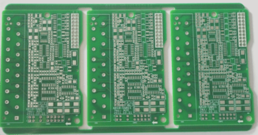
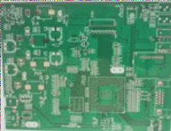
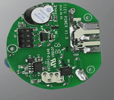
Key Steps in Multi-Layer PCB Fabrication Process
1. Initiate CNC drilling using the pre-designed positioning system. After drilling, etch and de-drill the hole walls before moving on to the double-sided plated hole PCB process.
Differences in Production Processes
2. When comparing multi-layer board and double-sided board production processes, unique steps for multi-layer boards include inner layer imaging, blackening, lamination, etch back, and de-drilling. Variations in process parameters, equipment accuracy, and complexity exist. For multi-layer boards, the inner metallization connection is crucial for reliability, leading to stricter hole wall quality requirements and elevated drilling needs.
Variances in Drill Bit Parameters and Inspection Protocols
3. The number of stacks per drilling for multi-layer boards and the drill bit’s speed and feed rate differ from those of double-sided boards. Inspection protocols for finished and semi-finished multi-layer boards are more stringent and complex. The glycerin hot-melt process, ensuring uniform temperature, replaces the infrared hot-melt process in multi-layer boards.
Advancements in Electronic Technology
4. Multi-layer PCB circuit boards represent the advancement of electronic technology towards high speed, multi-functionality, increased capacity, and reduced volume. WellCircuits Limited, a leading manufacturer in multi-layer PCB processing, is dedicated to enhancing production processes to drive progress in the electronics manufacturing sector.